Anyone who has disassembled a failing industrial remote control, handheld transceiver, or medical instrument after two years of heavy use has seen the same mysterious symptom: a greasy, transparent liquid film coating the gold PCB contact fingers directly beneath the rubber keypad, causing buttons to require hard mashing before they register. Maintenance technicians often blame ‘spilled coffee’—even inside hermetically sealed IP67 enclosures where no external liquid could possibly enter.
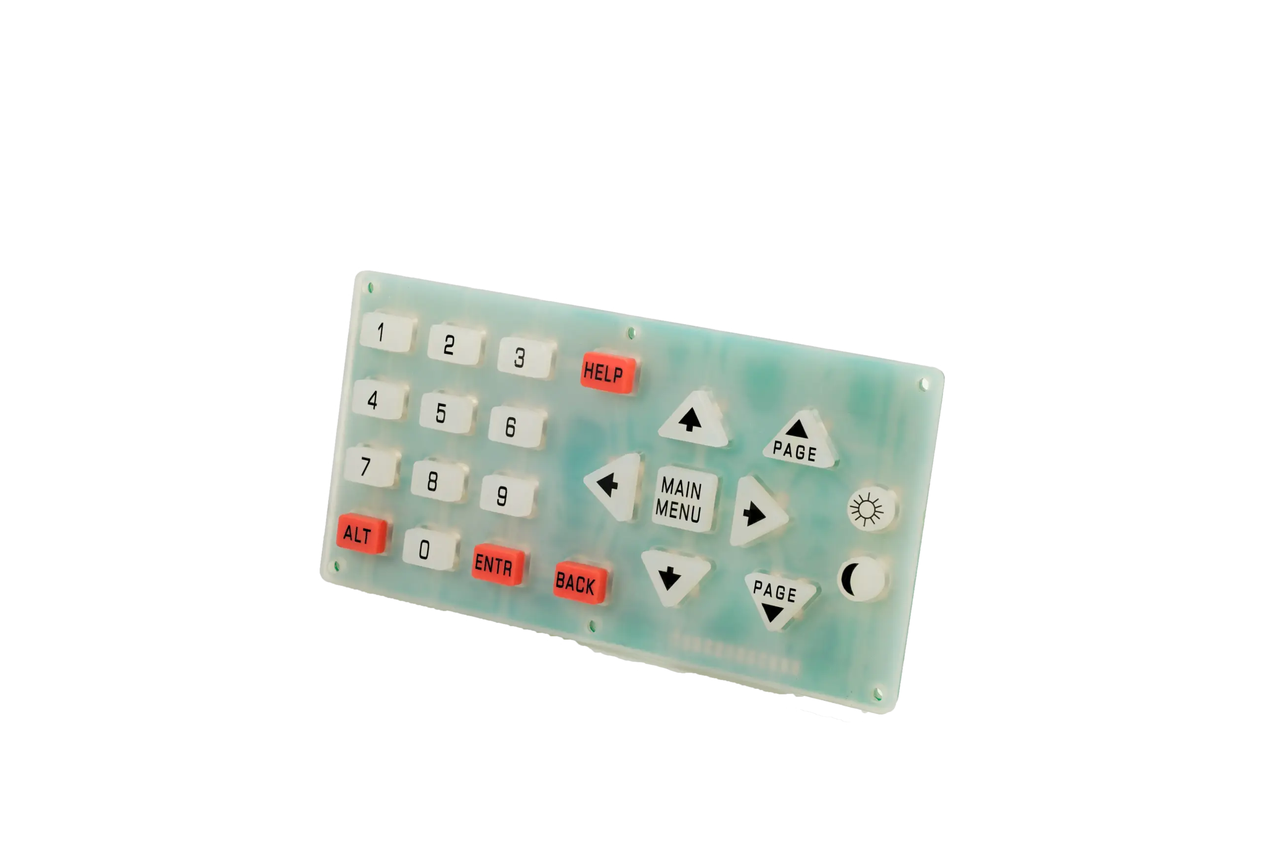
In elastomer engineering, that mysterious fluid is Silicone Oil Bleeding (Low-Molecular-Weight Cyclic Siloxane Migration, D4–D8). When a keypad manufacturer skips high-temperature Secondary Post-Cure Baking (200 °C × 4 hours) after compression molding, uncrosslinked siloxane oligomers slowly sweat out of the silicone web and form an insulating dielectric film across the conductive carbon pill and PCB pads. Here is how JASPER manufactures zero-bleed conductive rubber keypads that achieve >1,000,000 reliable actuations.
1. The Chemistry of Silicone Oil Bleeding — Why 200 °C Secondary Post-Curing Is Mandatory
Compression-molded silicone keypads are vulcanized at 165 °C–175 °C for 180–300 seconds using peroxide or platinum-addition catalysts. When the keypad comes out of the steel mold, 1.5% to 2.5% of the polymer mass consists of volatile, short-chain cyclic dimethylsiloxane oils (D4, D5, D6) and catalyst byproducts.
If a factory trims and packs those keypads immediately after molding to save oven electricity, those volatile siloxanes migrate to the surface over 6 to 18 months—especially when warmed by PCB electronics (40–60 °C). Worse, if a low-resistance switch arcs even slightly, siloxane vapor polymerizes into hard silicon dioxide (SiO2 glass) right on the contact pads! At JASPER, 100% of our silicone rubber keypads undergo mandatory 200 °C × 4-hour ventilated convection post-cure baking, driving off volatile siloxanes completely and stabilizing dimensional shrinkage before screen printing or laser etching.
2. Contact Pill Selection: Conductive Carbon Pills vs. Gold-Plated Pills vs. Nickel Pills
As outlined in our resource guide What Is a Silicone Rubber Keypad?, the conductive element vulcanized into the underside of each rubber key determines its contact resistance, current capacity, and PCB finish requirements:
|
Contact Pill Type |
Contact Resistance ( |
Max Current & Voltage |
Mating PCB Pad Requirement & Ideal Application |
|
1. Molded Conductive Carbon Pill (Standard) |
|
<= 10 mA at 3.3–5.0 V DC |
Mates with ENIG ( |
|
2. Gold-Plated Brass / Copper Pill ( |
|
Up to 50–100 mA at 5–24 V DC. |
Mates with ENIG Gold PCB pads. Mandatory when circuit requires ultra-low contact resistance, analog voltage-divider ladders, or direct LED switching. |
|
3. Conductive Nickel / Silver-Filled Silicone Ink |
|
<= 20 mA at 3.3–5.0 V DC. |
Used on ultra-thin keypads (<0.8 mm travel) where a 0.5 mm thick molded pill cannot fit. |
|
4. Non-Conductive Actuator Post (Over Metal Dome / Tactile Switch) |
Determined by PCB switch (<0.5 Ω). |
Up to 100 mA+. |
Silicone pad acts as a 3D waterproof elastomer boot pressing a sealed stainless metal dome or SMT tact switch (Silicone Keypad Assemblies). |
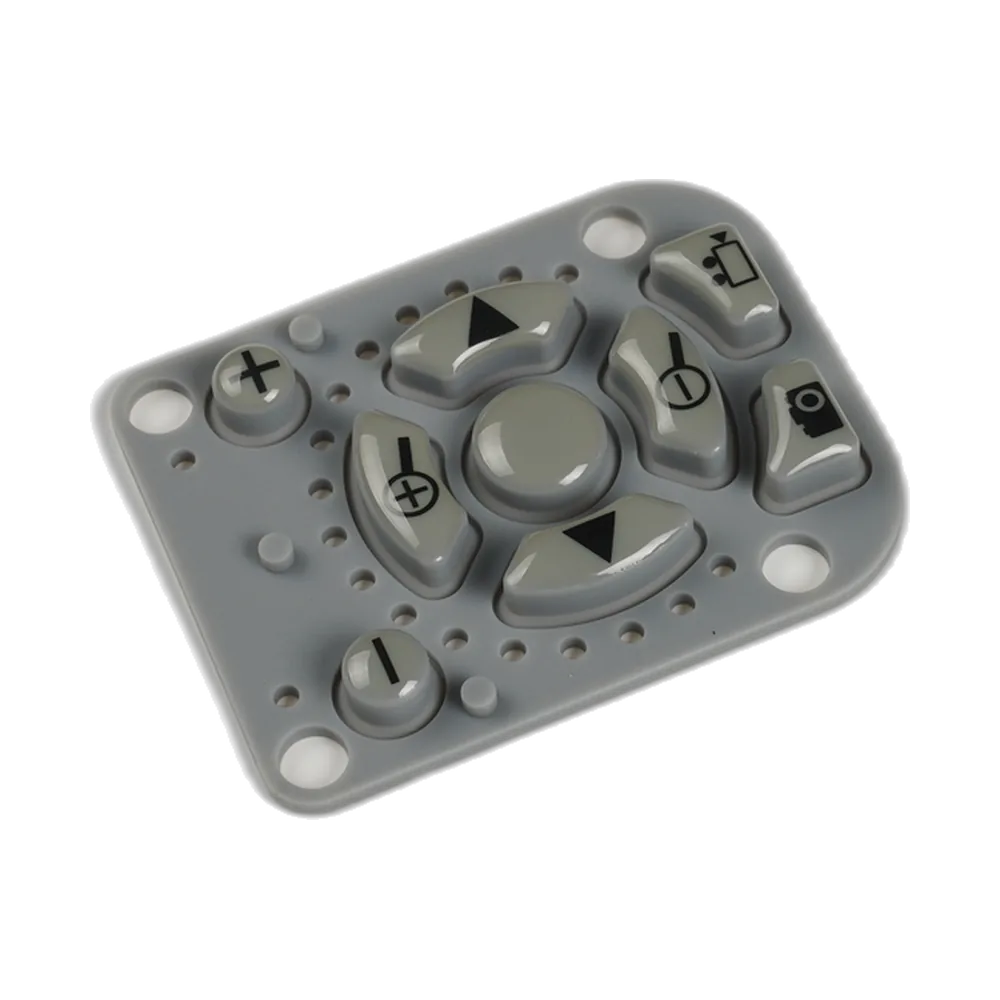
3. Designing the PCB Interdigitated Contact Footprint and Silicone Webbing Geometry
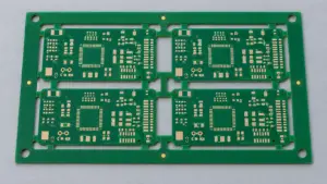
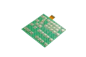
A conductive silicone keypad is only half of the switch—your underlying PCB forms the mating contact pair. To prevent missed presses when an operator pushes a button at an off-center angle, follow these three geometric rules:
- Use Concentric Circular or Serpentine Interdigitated Gold Fingers (Never Two Flat Half-Moons): Design an interdigitated comb pattern with
0.25–0.30 mmtrace width and0.25–0.30 mmair gap in ENIG (Electroless Nickel Immersion Gold) finish (never bare copper or uneven HASL solder!). - Size the Carbon Pill
1.0 mmLarger Than the Active PCB Comb Area: A Ø 3.5 mm or Ø 4.0 mm carbon pill should bridge at least 4 to 6 alternating finger pairs even under ±0.35 mm lateral assembly shift. - Include Bottom Venting Channels (
0.8 mm × 0.4 mm) Between Keys: We mold interconnected bottom air-equalization grooves between keys and add a 1.5 mm tall perimeter sealing rib around the outer border of the keypad mat to achieve IP65/IP67 enclosure sealing without separate O-rings.
|
Pre-RFQ DFM Checklist: 4 Silicone Keypad Rules for Mechanical & PCB Engineers • Specify Silicone Hardness and Web Geometry: 50–55 Shore A silicone with a 45° frustum cone wall angle (0.55 mm wall thickness) delivers the crispest 45%–55% tactile snap ratio. • [ ] Never Use Standard VMQ Silicone Below –40 °C Without Phenyl Modification: As explained in our Silicone Operating Temperature Guide, for arctic (-55 °C to -65 °C) applications, specify Low-Temperature Phenyl Silicone ( • [ ] Leave >= 0.30 mm Radial Clearance Between the Key Top and Enclosure Bezel Hole: A 10.0 × 10.0 mm rubber button requires at least a 10.6 × 10.6 mm bezel hole (0.30 mm gap per side) so the key never binds when pressed off-axis. • [ ] Add Guide Pins / Boss Holes Every 35–50 mm Across the Keypad Mat: Molded locating bosses (Ø 2.0–2.5 mm) pulled through matching PCB holes prevent the flexible rubber mat from bowing up in the center. |
Frequently Asked Questions (FAQ)
Q1: Why should I never use HASL (Hot Air Solder Leveling) on a PCB under a conductive rubber keypad?
HASL tin-lead or lead-free solder leaves uneven, dome-shaped bumps across fine interdigitated fingers and forms an insulating tin-oxide layer within months. Always specify flat ENIG (Immersion Gold) or Screen-Printed Carbon Ink over Copper on keypad PCBs.
Q2: How do you protect printed legends on silicone keypads from rubbing off?
We apply a sprayed Matte Polyurethane (PU) or Silicone Hard-Coat Topcoat (15–25 µm) tested to >100,000 cycles on a Norman RCA Paper-Tape Abrasion Tester (175 g load), or use permanent two-layer laser etching.
Q3: Can JASPER deliver a complete tested assembly with the silicone keypad, PCB, and plastic bezel?
Yes. Our Silicone Keypad Assemblies integrate the compression-molded keypad, ENIG/FPC circuit board, metal domes, LEDs, and adhesive/plastic frame into a single plug-and-play module.
Build Long-Life Conductive Silicone Keypads With JASPER
Need custom compression-molded or LSR silicone keypads with zero oil bleed and crisp tactile snap? Explore our Conductive Rubber Keypads or Request a Quote for a DFM review of your 3D STEP files.
Ready to Start Your Project?
Tell us about your membrane switch, keypad, or graphic overlay requirements. Our engineering team will review your specifications and provide a detailed quote.