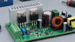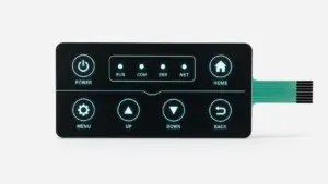
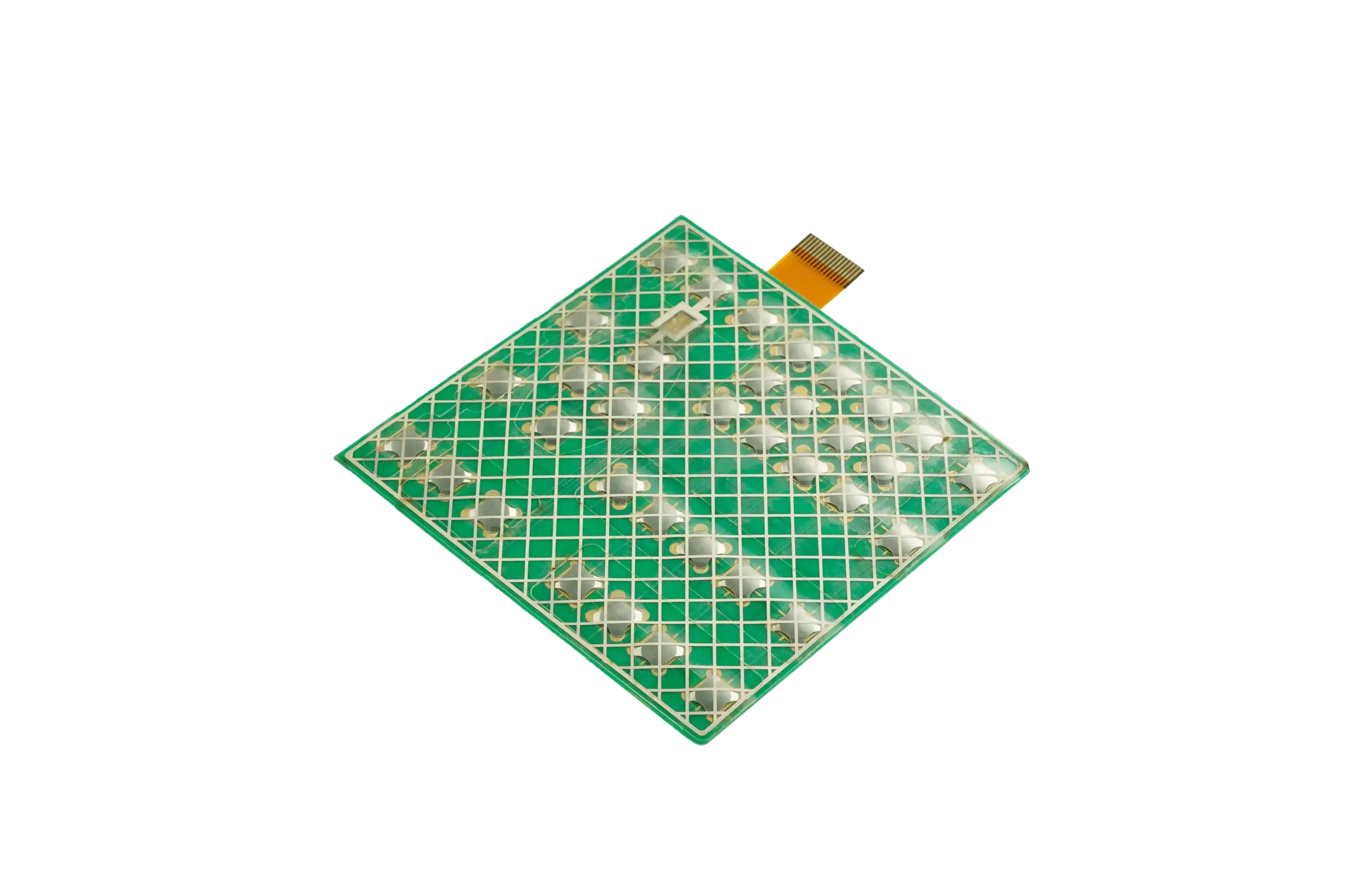
Few moments are more stressful for a hardware team than watching a new product fail IEC 61000-4-2 Electrostatic Discharge (ESD) compliance testing just weeks before mass production. When the test engineer fires an ±8 kV contact or ±15 kV air discharge gun at the front control panel—or when a user walking across a dry winter carpet or running on a commercial treadmill touches the START button—an unshielded membrane switch allows a high-current electrostatic arc (30 A peak in <1 ns) to jump straight into the microcontroller’s 3.3 V GPIO pins, causing instant MCU lockups, corrupted LCD characters, or blown CMOS inputs.
While PCB-level TVS diode arrays (PESD5V0 / USBLC6) help clamp conducted transients, **stopping a 15 kV spark after it has already entered your ribbon cable and radiated electromagnetic noise across your mainboard is often too late**. The most reliable solution is intercepting and shunting the electrostatic charge to chassis earth at the front surface using an ESD/EMI Shielded Membrane Switch. Here is how we engineer and ground shielded HMIs.
1. How a 15 kV Electrostatic Arc Breaches an Unshielded Keypad
A pristine 0.175 mm (7 mil) sheet of biaxially oriented polyester (PET) has a dielectric breakdown strength exceeding 160 V/mil (>1,100 V to 15,000 V depending on thickness and ink layers). So why does an ESD gun set to 8 kV or 15 kV effortlessly arc into the switch matrix?
- 1. Perimeter Edge Creepage & Display Window Seams: Air breaks down at approximately
3.0 kV per millimeter. A 15 kV electrostatic charge on a finger will jump across a 4.5 mm air gap around the outer perimeter of the graphic overlay, through a display window seam, or down a potentiometer shaft hole directly onto the internal silver matrix traces. - 2. Micro-Thinned Embossed Button Rims & LED Cutouts: Where the graphic overlay is stretched thin around a sharp embossed button rim—or where an internal spacer has a die-cut hole for an SMD LED or metal dome—the total dielectric barrier between the user’s finger and the live 3.3 V copper/silver trace drops to a single 0.15 mm film layer.
- 3. Capacitive Electric-Field Coupling (
dV/dt): Even when no physical spark punctures the film, a 15 kV discharge onto the surface of an unshielded overlay induces a massive capacitive displacement current (I = C × dV/dt) directly into the underlying matrix tracks.
2. Comparing the Four ESD & EMI/RFI Shielding Topologies
Depending on whether your panel requires electrostatic spark diversion (ESD), radio-frequency emission containment (EMI/RFI), or transparent LCD window shielding, JASPER integrates four distinct shielding layers directly beneath the graphic overlay:
|
Shielding Architecture |
Construction & Surface Resistivity |
ESD & EMI Attenuation Performance |
Best Application & Cost Impact |
|
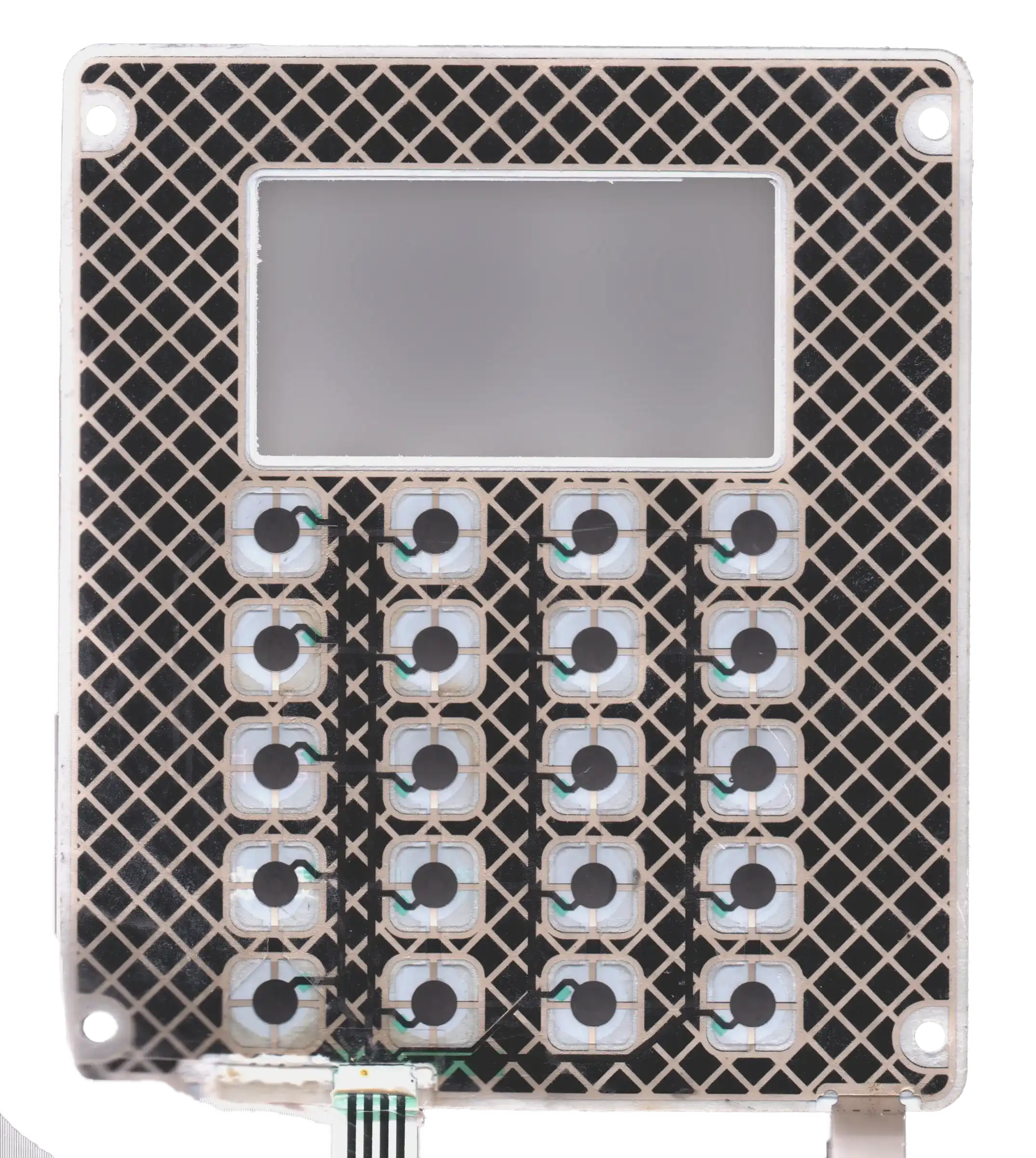
1. Printed Conductive Silver / Carbon Cross-Hatch Grid |
Dedicated 0.075–0.125 mm PET layer printed with a 50%–75% silver/carbon diamond mesh or solid flood (<0.5 Ω/sq). |
|
Most popular & cost-effective for treadmill switches, medical pumps, and industrial keypads. |
|
2. Laminated Aluminum Foil / Copper-Mylar Shield |
Continuous 0.025–0.050 mm aluminum or copper foil laminated to polyester with selective die-cut windows. |
|
High-frequency RF test instruments, military/defense radios, and noisy VFD inverter cabinets. |
|
3. ITO Transparent Film or Micro-Mesh Display Window Shield |
Indium Tin Oxide (ITO, 50–300 Ω/sq, >85% light transmission) or darkened stainless micro-mesh over LCD cutouts. |
Prevents ESD arcs and radiated EMI from entering/exiting large glass or acrylic display viewports. |
Medical patient monitors, spectrum analyzers, and Tempest-hardened enclosures. |
|
4. Perimeter Guard Ring (Single-Layer Economy Option) |
2.0–3.0 mm grounded silver/carbon guard trace printed around the outer border of the existing circuit layer. |
Intercepts edge-creepage sparks up to |
Budget-sensitive appliances and indoor controls needing basic edge-arc protection. |
3. The #1 Shielding Mistake: High-Inductance Grounding Through a Long ZIF Tail
Adding a conductive shield layer inside your membrane switch is useless if the shield is connected to ground through a narrow 0.5 mm silver trace running down a 150 mm long ZIF tail into your main logic board’s digital GND plane! Because an IEC 61000-4-2 ESD pulse has a rise time of 0.7 to 1.0 nanoseconds (equivalent to a 300 MHz+ RF transient), a narrow 150 mm tail trace exhibits roughly 120–150 nH of series inductance (L). At dI/dt = 30 A / 1 ns, the inductive voltage drop (V = L × dI/dt) exceeds 3,500 V—causing the ESD pulse to flash right over from the ground pin into the adjacent GPIO pins inside the ZIF connector!
To guarantee that ESD energy is shunted harmlessly away from your MCU, follow these three low-inductance chassis grounding rules:
- Bond the Shield Directly to the Metal Enclosure Chassis (
<20 nHPath): Instead of routing ESD current through the logic PCB, we extend a wide10–15 mmconductive grounding tab (or expose a 360° conductive adhesive window on the rear of the shield layer) that bonds directly to your unpainted aluminum subpanel or chassis ground stud via conductive acrylic PSA (3M 9703 / 9713). - If Grounding Through the Tail, Use Dual Wide Edge Pins Connected to
CHASSIS_GND(NotDGND): On plastic enclosures without a metal chassis, assign both outer pins (Pin 1andPin N) as 2.0 mm wide shield drains, and terminate them immediately at the ZIF connector footprint to a dedicated chassis/earth ring (CHASSIS_GND) coupled to digital ground via a high-voltage capacitor (1 nF–4.7 nF, 2 kV) and ferrite bead. - Keep the Shield Layer
1.5 mmInside the Outer Cut Edge: To prevent an external spark from jumping directly onto the exposed raw edge of the internal shield foil, we inset the shield perimeter 1.5–2.0 mm inside the graphic overlay’s 3M adhesive seal.
|
Pre-RFQ DFM Checklist: 4 Steps to Pass IEC 61000-4-2 & IEC 60601-1-2 on the First Try • [ ] Always Specify a Dedicated Top Shield Layer for Treadmills & Medical Devices: Walking on a treadmill belt generates continuous 5 kV–25 kV triboelectric charge, and IEC 60601-1-2 4th Edition mandates strict ±8 kV Contact / ±15 kV Air immunity for medical devices. • Keep the Shield Return Separate From the Button Matrix Common Bus: Never share the ESD shield return wire with your button matrix common bus! Sharing the wire injects a 30 A ESD spike straight into your MCU’s common pin. • [ ] Pair Membrane Shielding With 100 Ω – 1 kΩ Series Resistors + TVS Diodes on the PCB: A grounded membrane shield absorbs >90% of the discharge energy; placing a 220 Ω–470 Ω series resistor and low-capacitance TVS diode on each MCU matrix line clamps any residual induced spike. • [ ] Verify Shield Continuity ( |
Frequently Asked Questions (FAQ)
Q1: Does adding an ESD shield layer change the tactile feel of the buttons?
No. We place a ultra-thin 0.050–0.075 mm printed silver/carbon cross-hatch PET layer (or selectively perforated aluminum-mylar foil) directly beneath the graphic overlay and above the metal dome retainer. Because the shield layer is flexible and vented, dome actuation force and tactile snap remain identical.
Q2: Should the ESD shield layer be a solid silver flood or a cross-hatched diamond grid?
A 50%–70% cross-hatched diamond grid is superior over tactile key zones because it maximizes mechanical flexibility (>2,000,000 actuations), consumes less silver ink (lowering unit cost), and allows optical backlighting to pass through when needed, while still providing a tight Faraday cage against ESD arcs.
Q3: How do you ground an ITO transparent EMI shield over an LCD display window?
We print a 1.5–2.0 mm silver busbar frame around all four edges of the transparent ITO window film (outside the visible viewing area) and connect that busbar directly to the main panel ESD shield layer using Z-axis conductive adhesive (3M 9703).
Harden Your HMI Against ESD Resets & EMI Interference
Preparing for CE, FCC, UL, or IEC 60601-1-2 EMC laboratory testing? Explore our Shielded Membrane Switches and Treadmill Membrane Switches, or Request a Quote for a custom ESD-shielded stack-up.
Ready to Start Your Project?
Tell us about your membrane switch, keypad, or graphic overlay requirements. Our engineering team will review your specifications and provide a detailed quote.