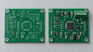
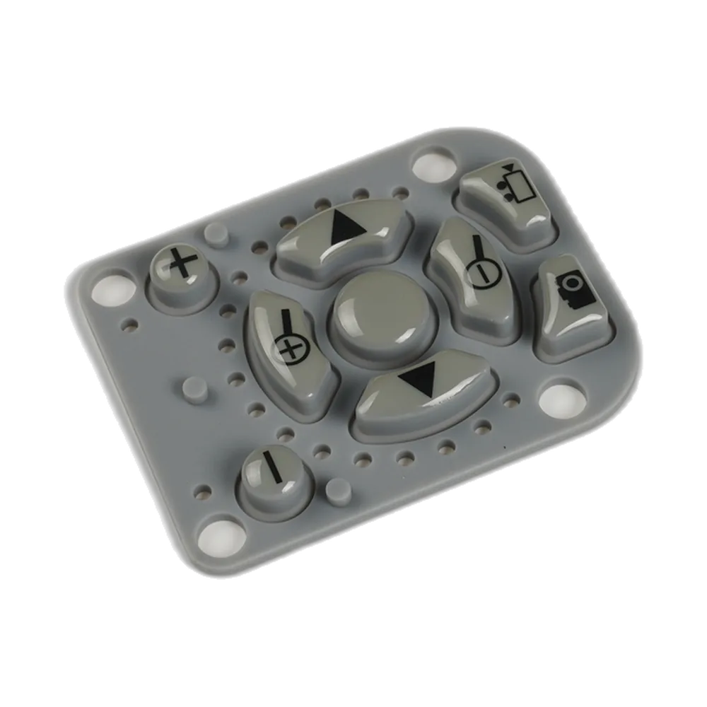
Conductive ink and molded conductive pills can both be used to close a rubber-keypad switch, but they are not interchangeable contact systems. A molded pill is a discrete conductive elastomer feature retained or integrated under the key. A printed conductive area is a cured conductive coating deposited on the silicone surface. The better choice depends on the actual material formulation, contact geometry, PCB interface, contact load, wear mechanism, environment, and inspection method—not on the label “ink” or “pill” alone.
For an OEM comparison, keep the mating circuit and test conditions the same, then compare the production-intent samples through initial electrical closure, mechanical travel, wear, contamination exposure, and lifecycle checks. A supplier change from a molded contact to a printed contact should therefore be treated as a design/process change that requires sample approval, not as a cosmetic substitution.
- Define the Two Contact Systems and Their Materials
- Compare Geometry and Process Controls
- Specify the Same Mating Circuit and Test Conditions
- Same-condition comparison record
- Review Wear, Adhesion, and Contamination Risks
- Approve Samples Before Changing the Contact System
- What to Send for a Contact-System Review
- Review Your Contact and Circuit Requirements
Define the Two Contact Systems and Their Materials
A molded conductive pill is a discrete conductive elastomer region attached to or molded into the underside of a silicone key. Conductive silicone can contain carbon or other conductive fillers and be formed into molded shapes. Material volume resistivity and the resistance of an installed switch are different properties; specify and verify the assembled contact path separately.
A printed conductive area is a coating system. Its performance depends on the conductive filler, binder, substrate preparation, deposited thickness, curing process, adhesion to silicone, and the way the coated area deforms during key operation. Depending on the supplier formulation, the conductive phase may be carbon-based, metal-filled, or a hybrid system. These categories should not share one assumed resistance, wear, cure, or adhesion value.
Research on conductive ink for silicone keypads found that formulation changes affected both electrical and adhesion/mechanical behavior, and identified durable adhesion to silicone as an engineering issue. The published results are not JASPER specifications, but they support qualifying the actual printed system rather than treating all inks as equivalent. See Zheng et al., Coatings (2022).
For a current molded-contact project, JASPER’s conductive rubber keypads page provides the commercial product context. Detailed circuit-resistance budgeting remains covered by the separate carbon-pill resistance guide.
Compare Geometry and Process Controls
The most useful comparison starts with how the conductive feature is created and controlled.
| Design / process question | Molded conductive pill | Printed conductive area | What the OEM should verify |
|---|---|---|---|
| Conductive feature formation | Discrete conductive elastomer geometry is molded, inserted, bonded, or otherwise retained under the key | Conductive ink is deposited as a defined area and cured on the silicone surface | Actual supplier process route and approved material system |
| Contact outline | Controlled by pill geometry and location | Controlled by artwork, printing method, edge definition, and registration | Worst-case overlap with both circuit electrodes |
| Thickness / height | Pill thickness and molded seat affect rest gap, first touch, and contact load | Printed film thickness and coverage affect surface profile and current path | How thickness is specified, measured, and sampled |
| Retention / adhesion | Mechanical or molded retention must survive handling, cycling, and environment | Coating adhesion must survive silicone flexing, contact rubbing, cleaning, and environment | Approved retention or adhesion evidence after relevant exposure |
| Contact surface | Molded surface may show texture, flash, edge damage, contamination, or local deformation | Printed surface may show pinholes, incomplete coverage, cure variation, cracking, abrasion, or edge lift | Visual criteria plus functional electrical criteria |
| Change control | Pill material, size, molding route, or retention change can alter the interface | Ink formulation, pretreatment, print thickness, cure, or artwork change can alter the interface | Which variables are locked after sample approval |
A printed contact can follow a custom outline, but the region still has to bridge the intended electrodes at worst-case keypad position and edge press. Registration, edge quality, silicone shrinkage, assembly location, and circuit tolerance remain part of the stack. For a molded pill, diameter, thickness, flatness, surface condition, location, and retention are natural drawing controls; a centered loose keymat still does not prove correct landing in the installed assembly.
Specify the Same Mating Circuit and Test Conditions
Do not compare one supplier’s printed contact on one PCB pattern with another supplier’s molded pill on a different fixture and call the result a material comparison. The mating circuit and loading conditions can dominate the measured switch behavior.
Use the same, production-intent definition for both candidate systems wherever the purpose is a direct A/B comparison:
- PCB/FPC/PET contact artwork and electrode gap;
- contact finish and cleanliness condition;
- keypad-to-circuit alignment and support;
- key actuation location, including center and relevant edge presses;
- force, travel, contact point, and permitted overtravel;
- electrical test voltage/current and measurement timing;
- sense points and fixture contribution;
- open-state, first closure, stable closed state, and release criteria;
- environmental preconditioning or contamination exposure; and
- lifecycle state when the measurement is taken.
Four-wire sensing can exclude lead-voltage drops when characterizing low resistance, but it is not mandatory for every keypad. If the requirement concerns the total switch path at the product connector, a controlled two-wire or functional test may be more relevant. Define one method and apply it consistently to both candidates.
Same-condition comparison record
| Item | Molded pill sample | Printed contact sample | Acceptance / observation |
|---|---|---|---|
| Contact geometry revision | Record | Record | Same mating circuit unless intentionally studying a redesign |
| Force/travel at first electrical closure | Measure | Measure | Project-defined |
| Stable closed-state resistance or circuit margin | Measure | Measure | Same electrical method |
| Intermittency / bounce during press and overtravel | Record | Record | Project-defined |
| Release / open-state behavior | Record | Record | Must reopen cleanly |
| Surface condition before test | Photograph / inspect | Photograph / inspect | Approved visual criteria |
| Condition after cycling / environment | Inspect and retest | Inspect and retest | Compare drift and failure mode |
This table is a validation template, not JASPER test data. The project still needs a controlled test plan and acceptance limits.
Review Wear, Adhesion, and Contamination Risks
The two systems can fail in different ways, so lifecycle inspection should look for different evidence.
For a molded pill, review whether the conductive element remains located and retained, whether its edge chips or tears, whether the surface polishes or becomes contaminated, and whether repeated off-axis presses change the contact footprint. Also inspect the mating PCB or printed circuit for localized wear or debris.
For a printed conductive region, add coating-specific checks: thinning, cracking, edge lift, delamination, adhesion loss after flexing, and changes after relevant cleaners or environment. Because the ink is a layer on silicone, adhesion and strain compatibility are part of the electrical design; an initial meter reading does not prove post-cycle stability.
Contamination matters to both systems. Define the contact-side and board-side cleanliness condition, and do not clean or precondition one sample set differently from the other. Neither architecture should be declared universally longer-lived; compare the actual failure modes on the intended circuit, load, support, environment, and duty profile.
Approve Samples Before Changing the Contact System
If an existing keypad uses molded pills and a supplier proposes conductive printing—or the reverse—treat the proposal as an interface change. At minimum, recheck geometry, force/travel at closure, electrical margin, PCB wear pattern, environmental exposure, and lifecycle drift.
A practical approval sequence is:
- Freeze the comparison boundary. Define the same circuit carrier, pad artwork, board support, housing stack, actuation method, and electrical test method.
- Document both contact constructions. Record the actual molded-contact material/process and the actual printed-ink system, including cure and any surface preparation.
- Inspect first articles. Check contact outline, location, surface condition, and any pill retention or print-adhesion evidence.
- Measure mechanical and electrical closure together. Relate first touch, first electrical closure, stable contact, overtravel, and release instead of recording only one static resistance number.
- Run the relevant wear and environment sequence. Use the project duty profile, not an invented universal cycle count.
- Retest and inspect failure evidence. Compare drift, intermittency, visual wear, adhesion/retention, contamination, and circuit-pad condition.
- Lock the approved process variables. A later change in ink formulation, cure, pretreatment, pill material, geometry, or retention method should trigger the defined change-control review.
When the OEM wants the circuit, support, lighting, connector, and final functional test controlled as one supplied module, a silicone keypad assembly can be reviewed as the validation boundary rather than approving a loose rubber part alone.
What to Send for a Contact-System Review
For a useful comparison or supplier-change review, submit the keypad drawing or 3D model, current contact specification, PCB/FPC/PET contact artwork, enclosure/support section, circuit schematic or input threshold information, force/travel target, intended environment, duty profile, known failure concern, annual quantity, and any current samples. If the ink type, pill material, lifecycle limit, or test method is not yet decided, mark it TBD rather than assigning a guessed value.
Review Your Contact and Circuit Requirements
If you are comparing conductive ink with molded pills for a new or existing keypad, request a keypad engineering review and include the contact drawing, mating circuit, mechanical stack, electrical criterion, environment, quantity, and the items that are still TBD. The review should confirm the actual material and process route before any resistance, wear, or life comparison is accepted.
Frequently Asked Questions
Is conductive ink the same thing as a carbon pill?
No. A carbon pill is a discrete conductive elastomer contact. Conductive ink is a deposited and cured coating. A carbon-based ink can contain carbon, but that does not make the printed layer a molded carbon pill.
Which contact system has lower resistance?
The manufacturing method alone does not answer that question. Resistance depends on the conductive formulation, geometry, contact force, PCB pattern and finish, contamination, measurement circuit, temperature, and lifecycle state. Compare the approved candidates under the same conditions.
Can a printed contact use the same PCB pad as a molded pill?
Possibly, but do not assume it. The contact footprint, thickness, surface, deformation, and worst-case alignment can change the useful overlap and pressure distribution. Recheck the PCB/FPC/PET pad pattern with the actual contact geometry.
How should a printed conductive contact be inspected?
Use project-specific visual and functional criteria. Typical review items include registration, coverage, pinholes or voids, edge condition, cured surface, thickness if it is a controlled characteristic, adhesion evidence, electrical closure, and condition after the required flex, wear, cleaning, or environmental exposure.
Can we switch from molded pills to conductive ink only to reduce cost?
Cost can be one input, but the change should not be approved from piece price alone. Requalify the mechanical/electrical interface, PCB compatibility, wear mode, inspection plan, and lifecycle behavior before releasing the new contact system.
Ready to Start Your Project?
Tell us about your membrane switch, keypad, or graphic overlay requirements. Our engineering team will review your specifications and provide a detailed quote.