A carbon-pill resistance specification should control the closed switch system,
not just the conductive rubber material. Separate material volume resistivity,
pill geometry, PCB pad geometry and finish, contact force, overtravel,
measurement circuit, contamination, environment, and lifecycle state. Measure
the production-intent key on the specified circuit and support, then verify open
state, closure, intermittency, bounce, release, and resistance drift before and
after cycling. One low reading from a loose pill does not prove that every
assembled key will switch reliably in the product.
JASPER’s conductive rubber
keypads
use a molded silicone key and a conductive element to close a circuit on PCB,
FPC, PET, or another contact structure. The quotation should state the circuit
threshold, resistance test method, pad definition, key load state, lifecycle
condition, and whether JASPER supplies the loose keymat or the tested assembly.
What Is a Conductive Carbon Pill?
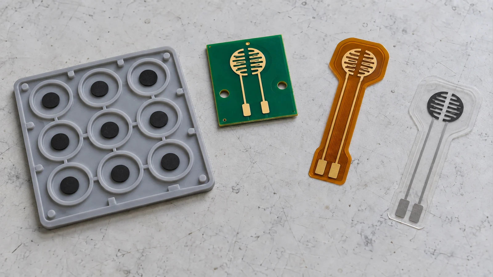
A conductive carbon pill is a molded or bonded conductive elastomer contact on
the underside of a silicone key. When the key moves far enough, the pill bridges
two electrically separate circuit pads and creates a conductive path.
The term carbon pill describes the contact component, not a guaranteed
resistance. Its result depends on:
- conductive filler and rubber formulation;
- pill diameter, thickness, flatness, and surface;
- molded retention and position;
- PCB pad pattern, finish, flatness, and cleanliness;
- contact force and available overtravel;
- key tilt and worst-case overlap;
- test voltage, current, timing, and sense points;
- temperature, humidity, chemicals, dust, and handling;
- cycling history and dwell; and
- circuit threshold and firmware behavior.
The electrical requirement belongs to the installed interface.
Separate the Resistance Quantities
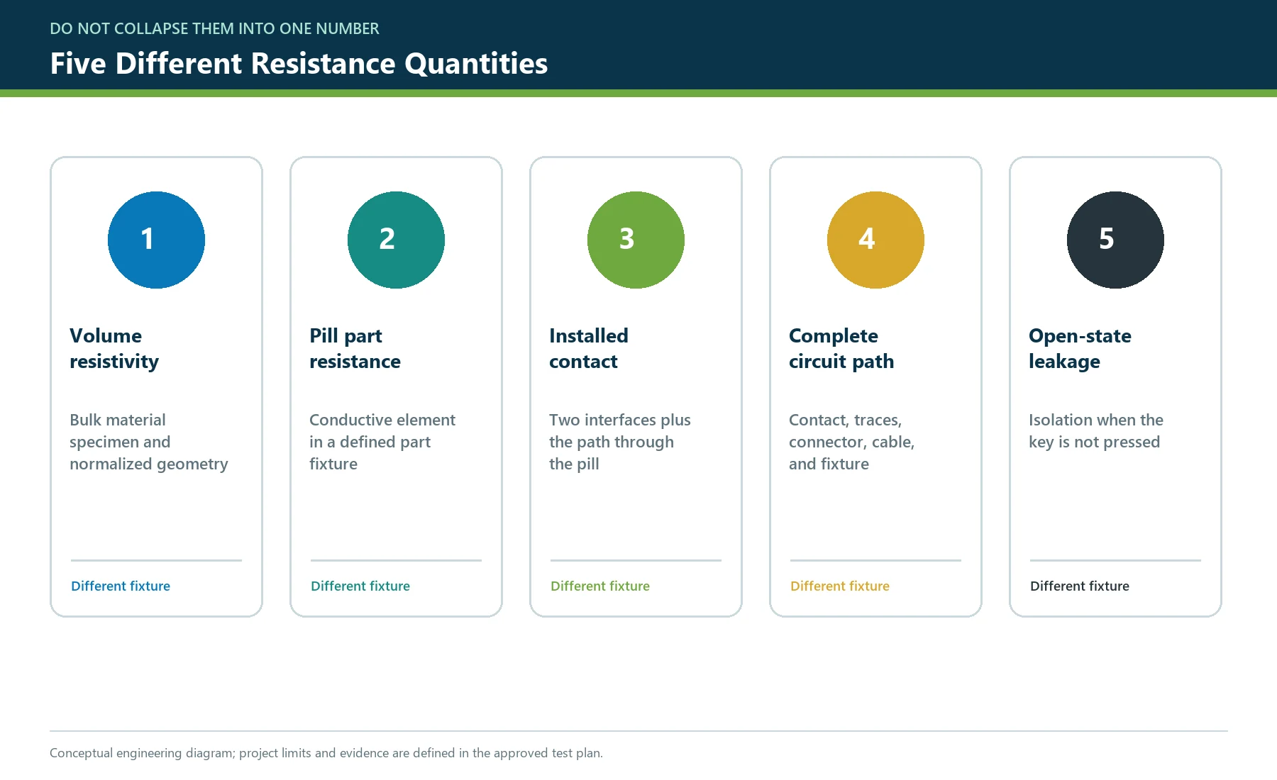
Several different values are often called carbon pill resistance.
| Quantity | What it describes | Why it cannot stand alone |
|---|---|---|
| Volume resistivity | Bulk conductive-rubber property normalized for specimen geometry | Does not include the real pill surface, PCB interface, pad pattern, force, or contamination |
| Pill part resistance | Resistance through or across one molded pill under a defined fixture | Fixture current path may differ from the installed two-pad bridge |
| Closed contact resistance | Resistance through the complete pressed pill-to-pad interface | Depends on force, overlap, pad finish, support, voltage/current, and measurement timing |
| Circuit path resistance | Closed contact plus PCB traces, connector, cable, fixture, and other series elements | May hide or exaggerate the contact contribution |
| Open-state resistance or leakage | Isolation when the key is not pressed | Answers accidental conduction and contamination questions, not closed-switch margin |
Volume resistivity describes a homogeneous conductor using the specimen length and cross-sectional area. ASTM D991 covers volume resistivity of conductive and antistatic rubber products. These material measurements are useful for compound control, but they do not replace an installed keypad contact test.
Model the Complete Closed Path
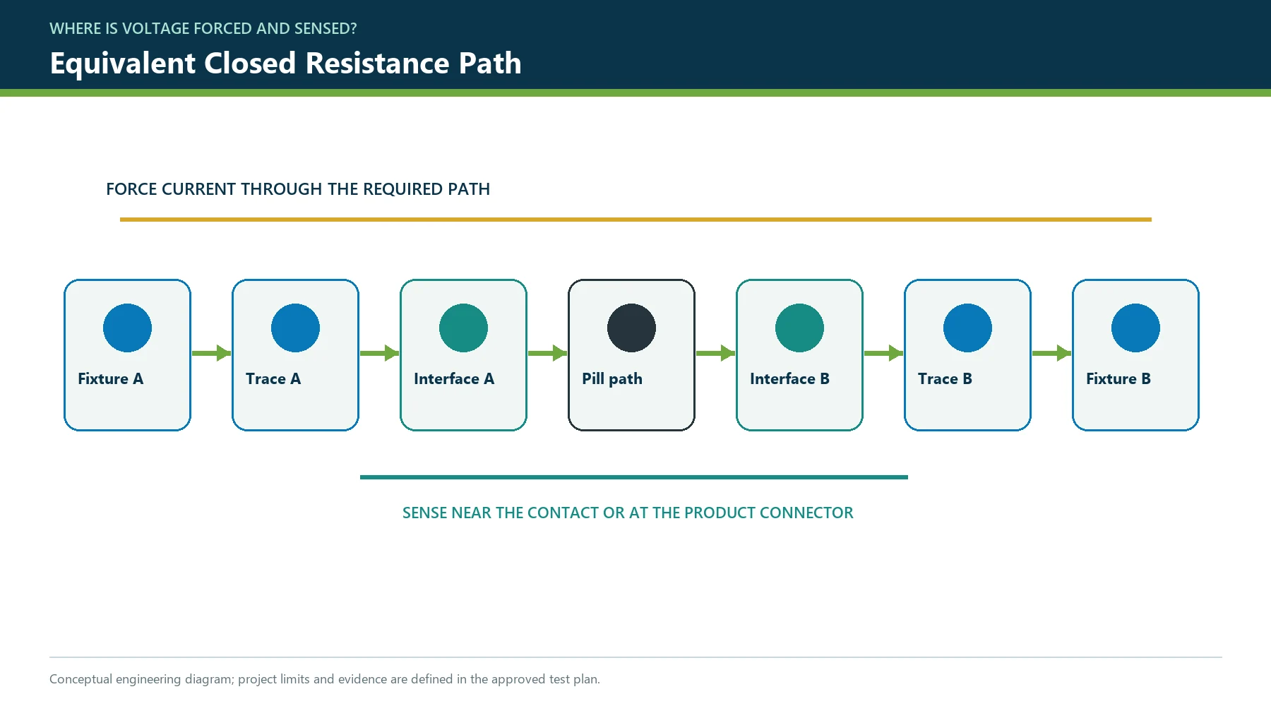
A simplified two-pad path is:
test lead or product trace A
        |
PCB pad A
        |
pill-to-pad interface A
        |
conductive path through the carbon pill
        |
pill-to-pad interface B
        |
PCB pad B
        |
test lead or product trace B
The measured resistance can be represented conceptually as:
Rmeasured =
  Rfixture
  + Rtrace_A
  + Rinterface_A
  + Rpill_path
  + Rinterface_B
  + Rtrace_B
This is a diagnostic model, not a promise that each term is constant or can be
isolated with a simple meter. Elastomer contacts can respond to force, surface
films, geometry, current, temperature, and time.
State where the voltage is sensed. A reading at the connector includes more of
the assembly than a reading at PCB test points beside the pads. Both may be
useful, but they answer different questions.
Derive the Resistance Limit from the Input Circuit
Do not begin with a generic contact-resistance number. Begin with the circuit
that decides whether the key is open or closed.
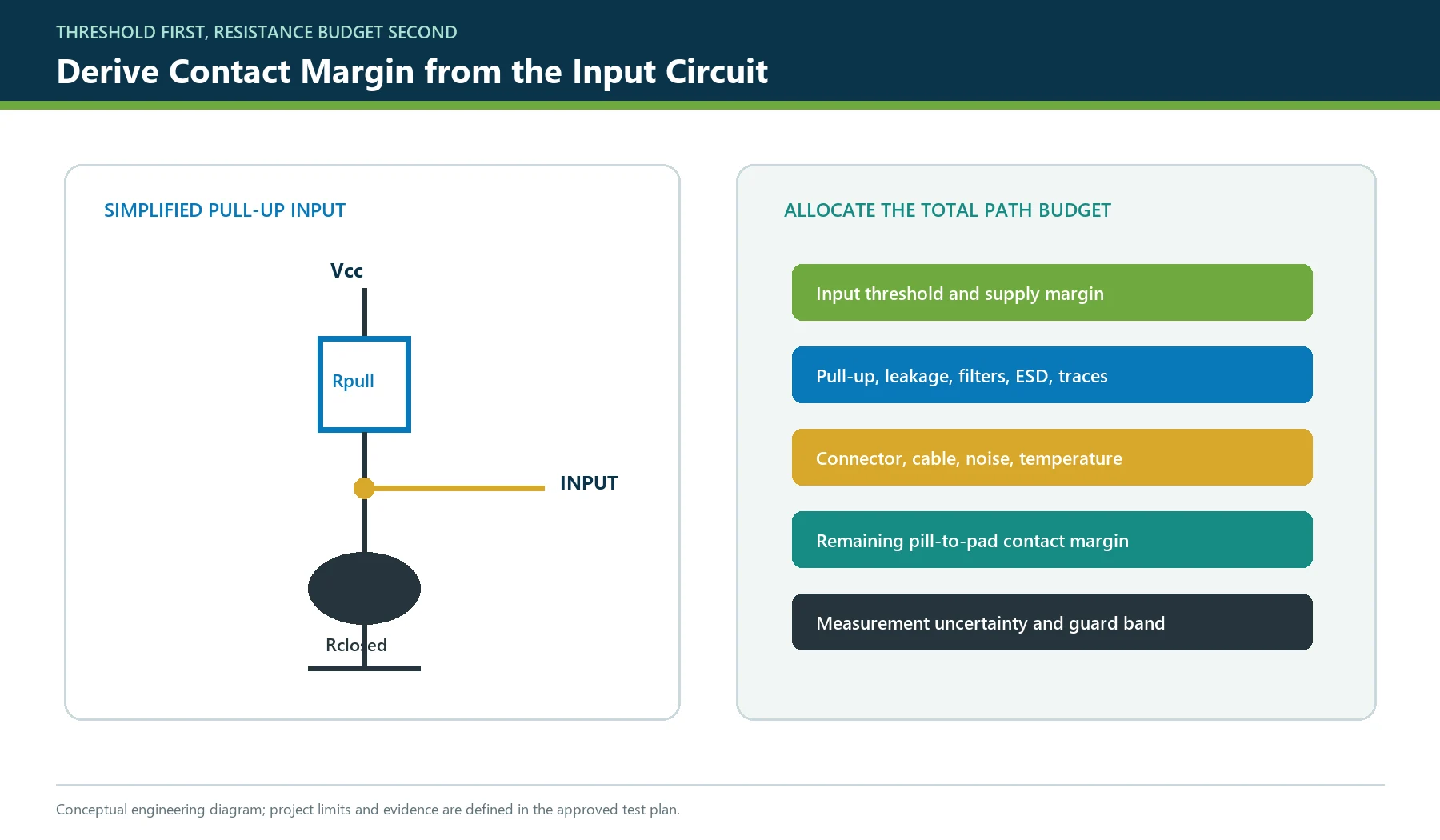
Digital input with a pull-up
For a simplified switch-to-ground input:
Vcc
 |
Rpullup
 |
 +------ input node
 |
Rclosed_total
 |
ground
Ignoring leakage and other error terms for the first calculation:
Vlow = Vcc x Rclosed_total / (Rpullup + Rclosed_total)
If the design team sets a conservative low-level target Vlow_target, the
idealized maximum path resistance is:
Rclosed_total <=
  Vlow_target x Rpullup / (Vcc - Vlow_target)
The released design must then include margin for:
- supply tolerance;
- pull-up tolerance;
- input-low threshold over temperature;
- input leakage;
- series resistors, filters, ESD parts, traces, connector, and cable;
- contact variation by key, cavity, lot, force, environment, and life;
- scan timing and settling;
- noise and ground shift; and
- measurement uncertainty.
The keypad contact receives only the portion of the path budget left after the
other series elements are counted.
Scanned keypad matrix
In a scanned matrix, define:
- which line is driven and which line is sensed;
- pull-up or pull-down values and tolerances;
- inactive-line state;
- scan rate and settle time;
- input thresholds;
- diode or isolation components, if present;
- cable and connector resistance;
- debounce algorithm; and
- fault behavior for two simultaneous keys.
Firmware debounce can reject short transitions. It cannot restore voltage margin
when the closed path is too resistive or unstable.
Analog or resistance-coded input
If the keypad forms part of an analog divider or resistor-coded network, contact
resistance becomes part of the measured code. Evaluate worst-case separation
between valid keys, ADC reference and input errors, resistor tolerance,
temperature, leakage, cable effects, and contact drift.
A carbon contact that is acceptable for a digital input may be unsuitable for a
precision analog measurement.
Current-carrying load
Do not route an LED, motor, solenoid, heater, or other significant load through
the pill merely because the contact closes during a meter check. Verify current,
voltage drop, heating, transient, fault energy, duty cycle, and material limits.
Use the keypad as a logic input with a separate driver when the load exceeds the
qualified contact function.
Contact Force Changes the Interface
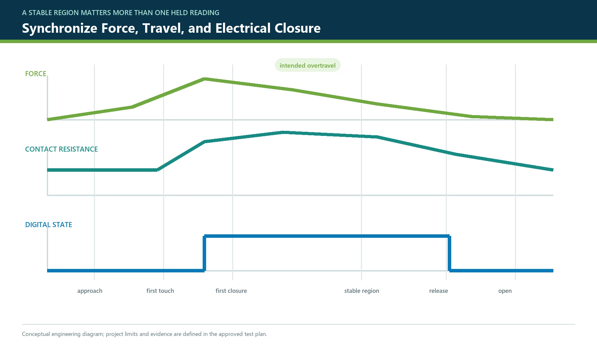
When the pill first touches the pad, the apparent contact area is smaller than
the full visible pill. Additional displacement can increase the number and size
of conductive microcontacts, change the current path, and stabilize closure.
The useful electrical trace should be synchronized with the mechanical
force-displacement trace:
key travel
   |
   +-- first physical touch
   |
   +-- first electrical closure
   |
   +-- stable closed region
   |
   +-- intended overtravel
   |
   +-- hard stop or bottoming
Record resistance during the stable closed region instead of using an
unspecified finger load. The key must also reopen cleanly on release.
Too little contact load can produce intermittent closure. Excessive load or
bottoming can increase wear, distort the pad, overload the PCB support, damage
the pill edge, or change the force feel. The correct window is established by
the production key, circuit, support, and enclosure.
Control Pill Geometry and Retention
Diameter and pad coverage
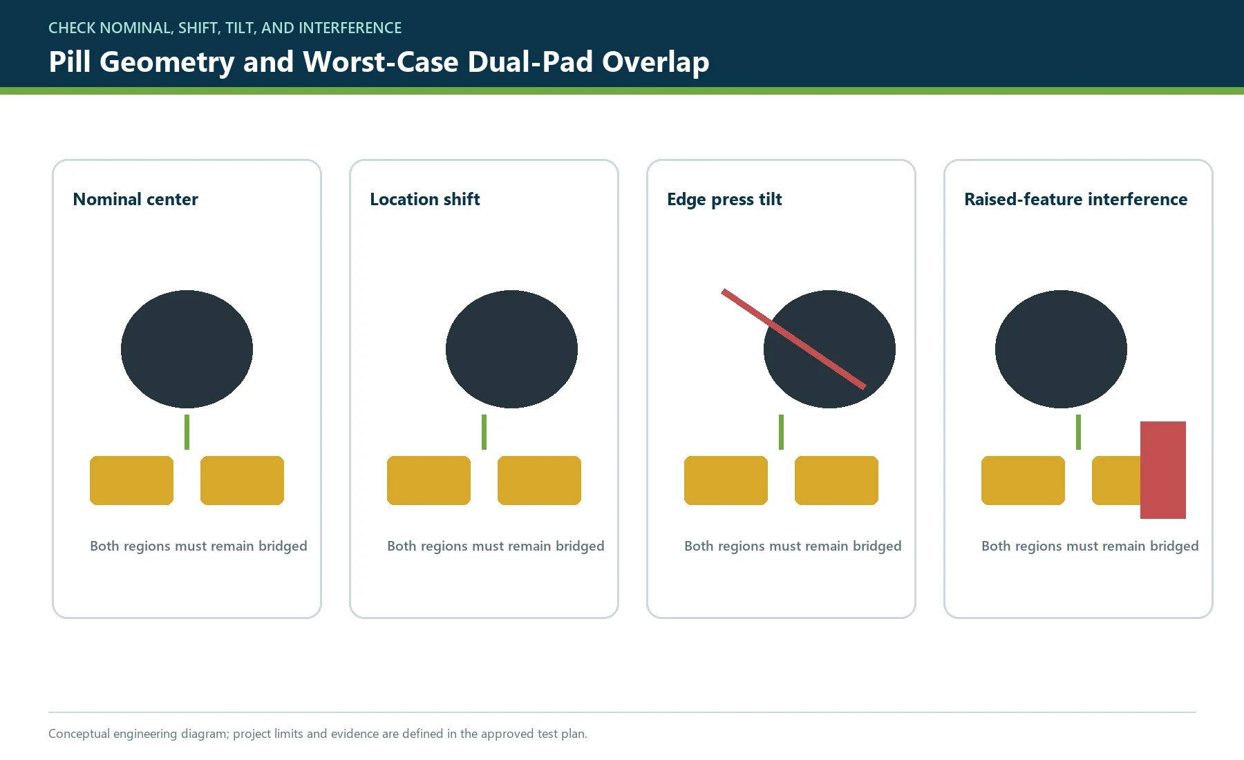
The pill must bridge the intended pad features at worst-case position. Its
diameter is not interchangeable with the PCB contact diameter because the pad
contains two separate electrical regions and a gap.
Check:
- nominal pill center;
- molding and assembly location tolerance;
- key tilt during center and edge press;
- PCB location tolerance;
- pad fabrication tolerance;
- housing and locator clearance;
- minimum overlap with both electrical regions; and
- clearance from solder mask, vias, components, and raised features.
Thickness and surface condition
Pill thickness influences the rest gap, first touch, contact load, overtravel,
and current path. Define whether thickness is controlled directly, by molded
geometry, or by an approved contact component.
Inspect:
- flatness or intended crown;
- molded flash;
- cuts, chips, tears, voids, or exposed nonconductive rubber;
- embedded contamination;
- surface gloss or texture when it affects the approved interface;
- edge condition; and
- orientation if the pill is not symmetric.
Retention
The pill must remain attached and located through molding, demolding, finishing,
handling, assembly, cycling, environment, and service.
Do not rely only on a visual pull at incoming inspection. Define the molded
retention feature, inspection evidence, destructive audit if appropriate, and
failure action when a pill shifts or separates.
Choose PCB Pad Geometry as a System Decision
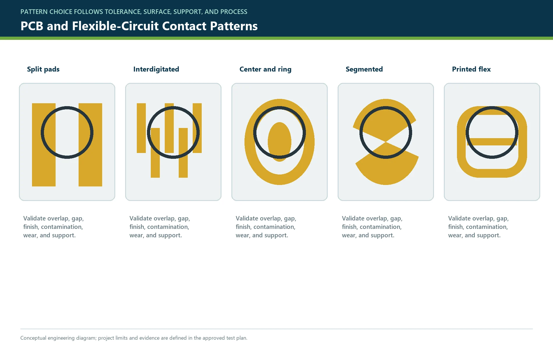
The pad must create two separate conductors that the pill bridges. Several
patterns are possible.
| Pad concept | Potential design reason | Main questions to validate |
|---|---|---|
| Two split pads | Simple current path and artwork | Does the pill overlap both sides across all tolerances and edge presses? |
| Interdigitated fingers | Multiple parallel contact regions within the footprint | Are finger width, gap, fabrication capability, contamination, and wear controlled? |
| Center-and-ring | Radial tolerance around a center feature | Does the pill contact both regions uniformly without shorting at rest? |
| Curved or segmented pattern | Fits a noncircular key or local routing | Does the real current path remain stable under tilt and partial contact? |
| Printed PET/FPC contact | Flexible or membrane-style circuit carrier | Are ink surface, thickness, cure, support, spacer, and environmental behavior qualified? |
The table identifies questions, not a preferred universal pattern.
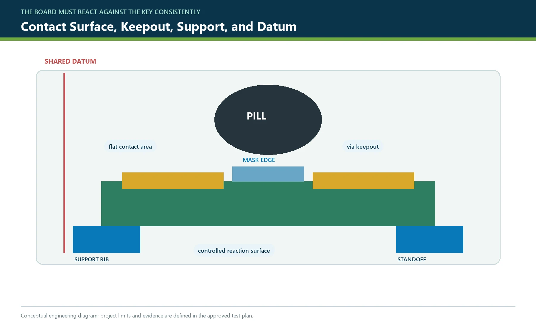
Keep the contact area flat and supported
Avoid uncontrolled surface steps inside the contact footprint. Review:
- solder mask edge and clearance;
- copper and plating thickness transition;
- via, via fill, or plug condition;
- trace entry;
- local board bow;
- component or solder-joint print-through;
- FPC or PET support;
- housing ribs and standoffs; and
- contamination traps.
The board or flexible circuit must have a controlled reaction surface beneath
the key. A pad that deflects away from the pill changes force, travel, and
resistance together.
Use a shared datum
Locate the pill and pad from shared keypad-to-PCB-to-housing datums. Do not
dimension the pill from an outside rubber edge while locating the PCB contact
from an unrelated enclosure wall without a tolerance chain.
Specify the Contact Surface, Not Just the PCB Finish Name
Pad finish affects surface condition, corrosion behavior, wear, fabrication,
cleaning, and repeatability. A finish family name is not enough to approve the
interface.
Record:
- exact contact-area build and supplier specification;
- final surface and any carbon or other coating;
- pad outline and permitted cosmetic condition;
- solder mask relationship;
- flatness and roughness requirement when relevant;
- cleaning and packaging method;
- prohibited rework, solder, flux, marker, adhesive, or handling in the area;
- shelf and storage controls; and
- change-notification requirement.
Do not replace a plated pad, carbon-coated pad, or printed contact with another
surface because its nominal conductivity looks similar. Requalify closure,
variation, environment, and life with the production pill.
Treat Contamination as an Electrical Variable
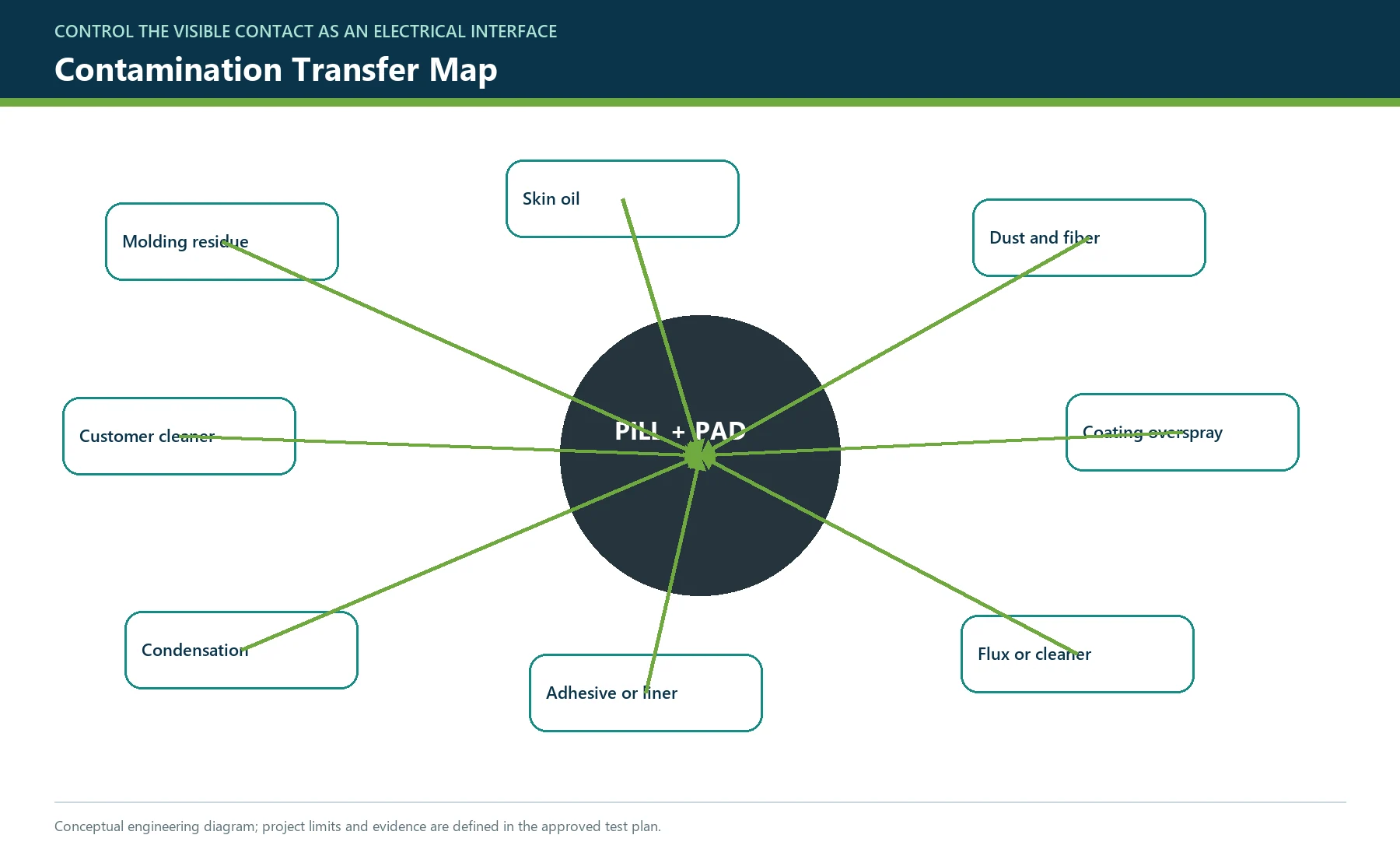
The visible contact area should be handled as a controlled interface.
Potential contaminants include:
- dust and fibers;
- skin oil and fingerprints;
- release-agent or molding residue;
- silicone oil or uncured material;
- coating overspray;
- laser or print residue;
- flux and board-cleaning residue;
- adhesive, foam, liner, or packaging particles;
- corrosion products;
- condensation and dried water residue;
- customer cleaner film; and
- lubricant transferred from housing assembly.
Keep the mating surfaces clean and control dirt, moisture, oil, solvents, and other contamination that can affect conductive-silicone properties. Validate the exact cleaning method on the selected pill, pad, coating, and circuit.
Do not introduce an unapproved solvent or abrasive wipe as an emergency fix. It
may change the pill surface, pad finish, resistance, life, or future
contamination behavior.
Build a Resistance Test Fixture Around the Real Stack
A useful fixture controls:
- keypad and circuit revision;
- key ID and cavity/lot identity;
- pill and pad position;
- PCB/FPC/PET support;
- enclosure or representative compression;
- press location;
- force or displacement endpoint;
- actuation and release rate;
- dwell before measurement;
- electrical source and sense points;
- voltage, current, polarity, and range;
- open-state threshold;
- measurement sample rate;
- temperature, humidity, and conditioning;
- fixture contact verification; and
- calibration and uncertainty.
If the product relies on the enclosure for support or preload, a loose bench
fixture is not the final acceptance configuration.
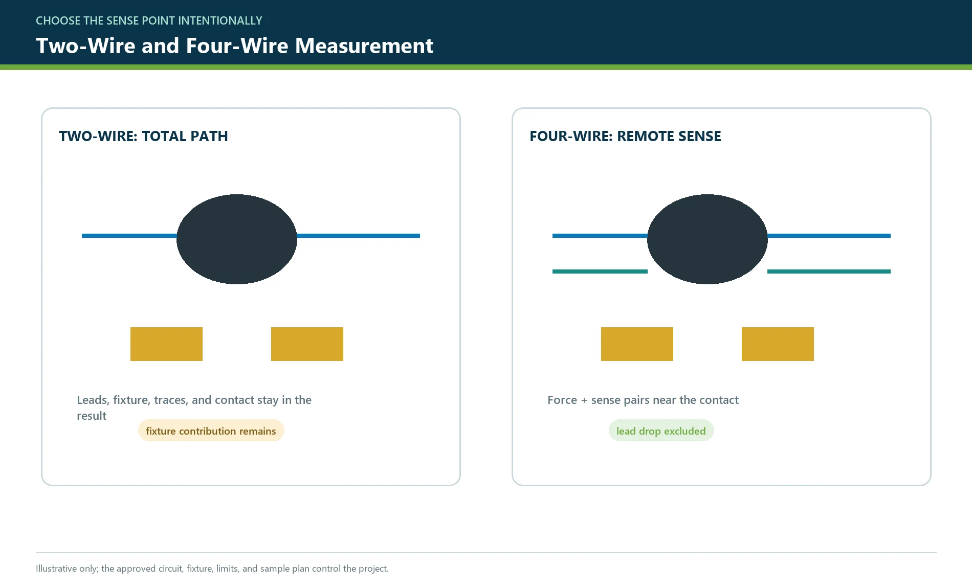
Choose Two-Wire or Four-Wire Measurement Intentionally
Two-wire measurement
Two-wire measurement includes test-lead, fixture, connector, trace, and contact
resistance in the reading. It may be appropriate when:
- the acceptance limit is well above the fixture contribution;
- the product is tested from its external connector;
- the total assembly path is the actual requirement; and
- fixture resistance is stable, checked, and included in the limit.
It becomes misleading when the fixture consumes a material share of the
resistance budget or drifts between stations.
Four-wire or Kelvin measurement
In a four-wire measurement, current is forced through one pair of conductors and voltage is sensed through another pair near the device under test. This remote-sensing arrangement excludes the lead-resistance voltage drop between the source and sense points from the measured voltage.
For a keypad, define whether the sense points are:
- beside the PCB contact pattern;
- at board test pads;
- at the connector;
- across a complete matrix route; or
- on a dedicated contact coupon.
Four-wire measurement does not remove the pill-to-pad interfaces. Those are the
subject of the test.
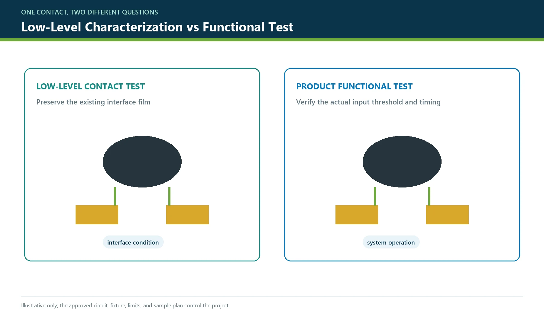
Separate Low-Level Contact Testing from Functional Testing
IEC 60512-2-1 defines a contact-resistance test at millivolt level for
electromechanical components. The low-level principle is designed to measure
the contact without electrically breaking through surface films.
Dry-circuit testing must avoid disturbing the contact interface: excess test voltage can puncture an oxide or film and produce an artificially lower result.
Use two explicit test purposes:
| Test purpose | Electrical condition | Question answered |
|---|---|---|
| Low-level contact characterization | Limited energy selected to preserve the existing interface film | What resistance does the undisturbed contact interface present? |
| Product functional test | Actual or representative circuit voltage, current, timing and thresholds | Does the complete keypad input work in its product circuit? |
One test does not automatically replace the other. If the drawing cites an IEC,
ASTM, customer, or internal method, state the edition, fixture, circuit,
conditions, and deviations.
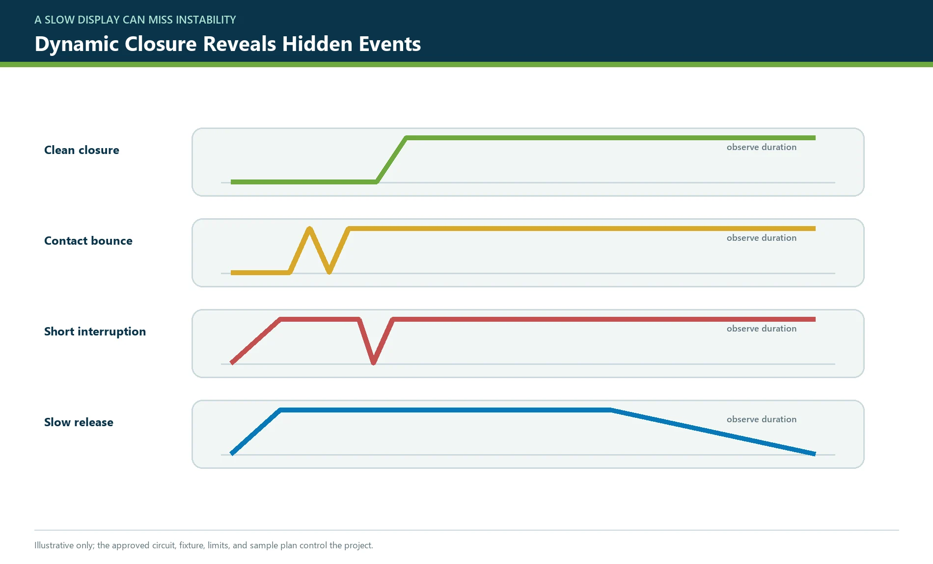
Capture the Dynamic Closure Rather Than a Static Number
A single reading after the operator holds the key can miss:
- delayed closure;
- brief opens during travel;
- multiple transitions;
- resistance spikes;
- bounce;
- unstable edge press;
- slow release;
- a key that closes only near hard bottoming; and
- a key that remains partially conductive after release.
Record synchronized channels when the project risk requires them:
time
 |-- force or displacement
 |-- contact voltage
 |-- contact current
 |-- calculated resistance
 |-- digital input state
Define the observation window, bandwidth, sample rate, threshold, and event
logic. A slow meter display cannot characterize short interruptions.
Write a Repeatable Test Sequence
An example project sequence is:
- identify sample, key, cavity, lot, keypad revision, circuit revision, and
fixture revision; - condition the sample as specified;
- verify fixture open and short checks;
- record open-state resistance or leakage;
- press at the defined location and rate;
- record first closure, stable closed region, force/travel, and resistance;
- hold for the defined dwell;
- release and record reopen behavior;
- repeat center and required edge/corner presses;
- run the specified number of preconditioning operations;
- repeat across key groups and samples;
- retain raw traces, summary statistics, failures, and deviations.
The sequence is a framework. Production settings require JASPER and customer
approval.
Define Acceptance Across the Product Life
Use an acceptance matrix rather than one undifferentiated maximum.
| Stage | Required checks | Why it matters |
|---|---|---|
| Initial molded sample | Pill position, surface, force/travel, closure, static and dynamic resistance | Establishes design feasibility |
| Decorated/assembled sample | Same checks with coating, circuit, enclosure, preload, connector, and lighting | Detects stack effects |
| Production qualification | Multiple samples, cavities/lots, fixture repeatability, environment and cycling | Establishes controlled release evidence |
| Production lot | Defined sampling or full functional test, open/short, resistance and visual checks | Controls shipment risk |
| Post-environment | Resistance, closure, release, corrosion/contamination and physical inspection | Detects exposure-related drift |
| Post-lifecycle | Resistance distribution, intermittent events, wear, force shift and failure mode | Tests duty-profile durability |
| Change qualification | Repeat affected tests after material, pill, pad, finish, tool, process, supplier or fixture change | Prevents silent interface changes |
The specification should state:
- initial and aged limits;
- per-key or key-group limits;
- statistical and absolute limits;
- permitted intermittent events;
- open-state minimum or leakage limit;
- bounce or settling requirement when relevant;
- test-current and voltage window;
- sample quantity and failure action;
- retest policy;
- raw-data retention; and
- responsibility for failure analysis.
Do not average away a failed high-use key.

Build Lifecycle Tests from the Real Duty Profile
Define:
- which keys are cycled;
- use frequency by key;
- center versus edge load;
- force or displacement endpoint;
- cycle rate and dwell;
- complete press and release;
- circuit voltage/current during cycling;
- powered or unpowered state;
- temperature, humidity, dust, cleaner, oil, UV, or condensation exposure;
- periodic resistance, force, travel, and visual checks;
- rest or recovery intervals;
- failure definition; and
- post-test disassembly.
Cycle count alone is not a complete life test. A fast laboratory press at one
load can produce a different failure mode from a slow gloved edge press in the
installed enclosure.
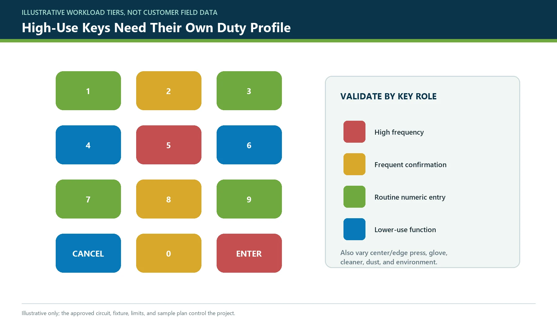
Track High-Use Keys Separately
Numeric access-control keypads, enter/cancel keys, navigation arrows, power
keys, and frequently used machine controls do not share the same field duty.
The existing security and access-control
application
page identifies repeated use, protected legends, night operation, environment,
and enclosure integration as application questions. For a carbon-pill design,
translate those questions into:
- per-key use distribution;
- worst-case high-use key cycling;
- glove or finger edge-loading;
- ingress and contamination exposure;
- powered measurement during use;
- resistance and bounce trend by interval;
- legend and surface wear;
- enclosure vandal/tamper load boundary; and
- field fault detection.
The application page is not evidence of a passed carbon-pill life test. The
project still needs its own duty profile and acceptance plan.
Use Manufacturing Data to Control Drift
The JASPER testing and quality-control
page describes drawing-based
continuity, short/open, actuation, visual, dimensional, adhesion, assembly, and
packaging checks for current membrane-interface work. SK-02 requires a more
specific conductive-keypad plan before publication.
Potential control fields include:
- key and pill ID;
- mold cavity;
- material and pill lot;
- molding and cure/post-cure record;
- pill location and dimensions;
- keypad force/travel;
- PCB/FPC/PET supplier and lot;
- pad artwork and finish revision;
- cleaning and handling record;
- assembly fixture and operator/station;
- resistance fixture and calibration;
- initial and final electrical result;
- defect/rework disposition; and
- retained sample location.
Look for distribution shifts as well as failures beyond a limit. A gradual move
can reveal fixture wear, contamination, pad change, material change, or process
drift before the product fails functionally.
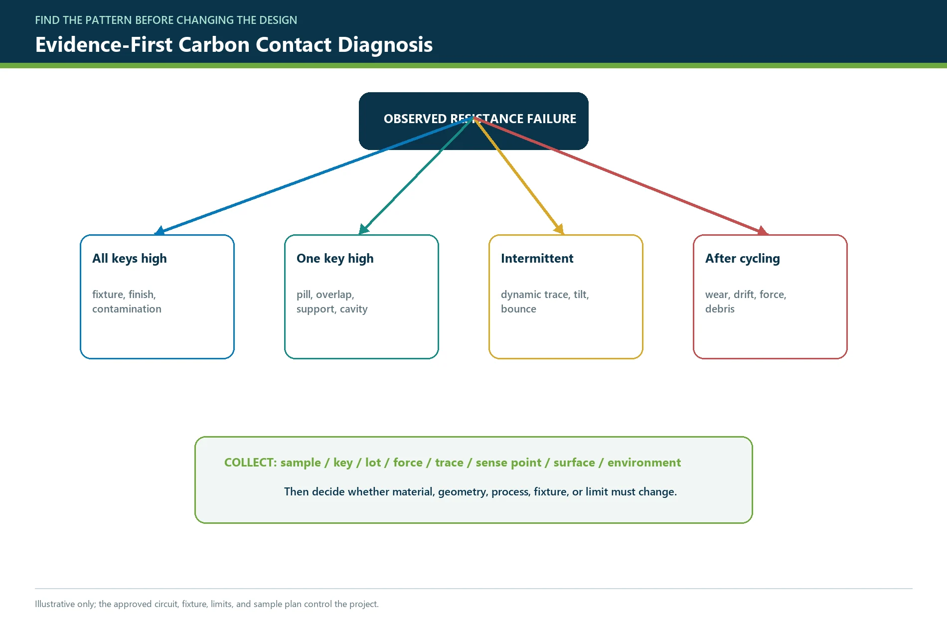
Diagnose Resistance Failures from Evidence
| Symptom | Possible causes | Evidence to collect first |
|---|---|---|
| High resistance on every key | Fixture, test settings, circuit finish, contamination, wrong material/lot | Fixture short, source/sense settings, lot map, surface inspection |
| High resistance on one key | Pill position, local contamination, pad defect, unsupported board, damaged web | Key/pill/pad alignment, local support, dynamic trace |
| Intermittent closure | Low overlap, tilt, insufficient overtravel, board flex, particles | Center/edge traces, force/travel, high-speed voltage record |
| Good loose sample, bad assembly | Enclosure preload, support change, PCB bow, locator shift, fastener sequence | Loose versus installed curves and resistance |
| Resistance rises during dwell | Viscoelastic movement, unstable force, heating, surface behavior | Force and resistance versus time, current, temperature |
| Resistance falls only at high test energy | Surface film electrically disturbed by the measurement | Low-level versus functional test comparison |
| Initial pass, post-cycle failure | Pill/pad wear, debris, force shift, retention loss, corrosion | Interval trend, microscopy/inspection, post-test disassembly |
| Slow or incomplete release | Preload, side rub, contamination, damaged web, pill sticking | Release curve, open-state trace, housing clearance |
| Key remains conductive at rest | Compressed stack, debris bridge, circuit contamination, damaged pill | Open resistance, disassembly, pad and pill inspection |
Do not polish, scrape, solvent-wipe, or replace the pad before documenting the
failure state. That can erase the evidence.
Know When a Carbon Pill Is the Wrong Contact
Review another contact architecture when:
- the circuit needs very low or tightly controlled resistance;
- significant load current must pass through the key;
- analog accuracy cannot tolerate contact variation;
- the contact must switch a signal outside the qualified electrical range;
- available footprint cannot provide robust overlap;
- the environment cannot be controlled at the exposed pad;
- service requires a field-replaceable sealed switch;
- the PCB support cannot be made stable; or
- the product already uses qualified mechanical switches or metal domes.
Alternatives may include a metal pill, metal dome, board-mounted switch,
separate sealed switch, or a different sensor architecture. They introduce
their own force, plating, bounce, sealing, cost, assembly, and lifecycle
questions.
Decide the Supplied Test Boundary
If JASPER supplies only the rubber keymat, the customer owns more of the contact
evidence because the final PCB, finish, support, enclosure, connector, and
electronics remain outside the shipment.
The silicone keypad
assembly
route can place the keymat, circuit, support, LEDs, connector, and functional
test inside one supplied module. The parties must still define:
- whether resistance is measured at pad test points or the external connector;
- which fixture represents the enclosure;
- who owns firmware and input thresholds;
- which parts are customer-supplied;
- how failures are traced to key, pill, pad, circuit, or assembly; and
- which changes require requalification.
For the mechanical prerequisite, use the silicone rubber keypad design guide to release key geometry, force, travel, support, and the installed stack before assigning the contact-resistance limit.
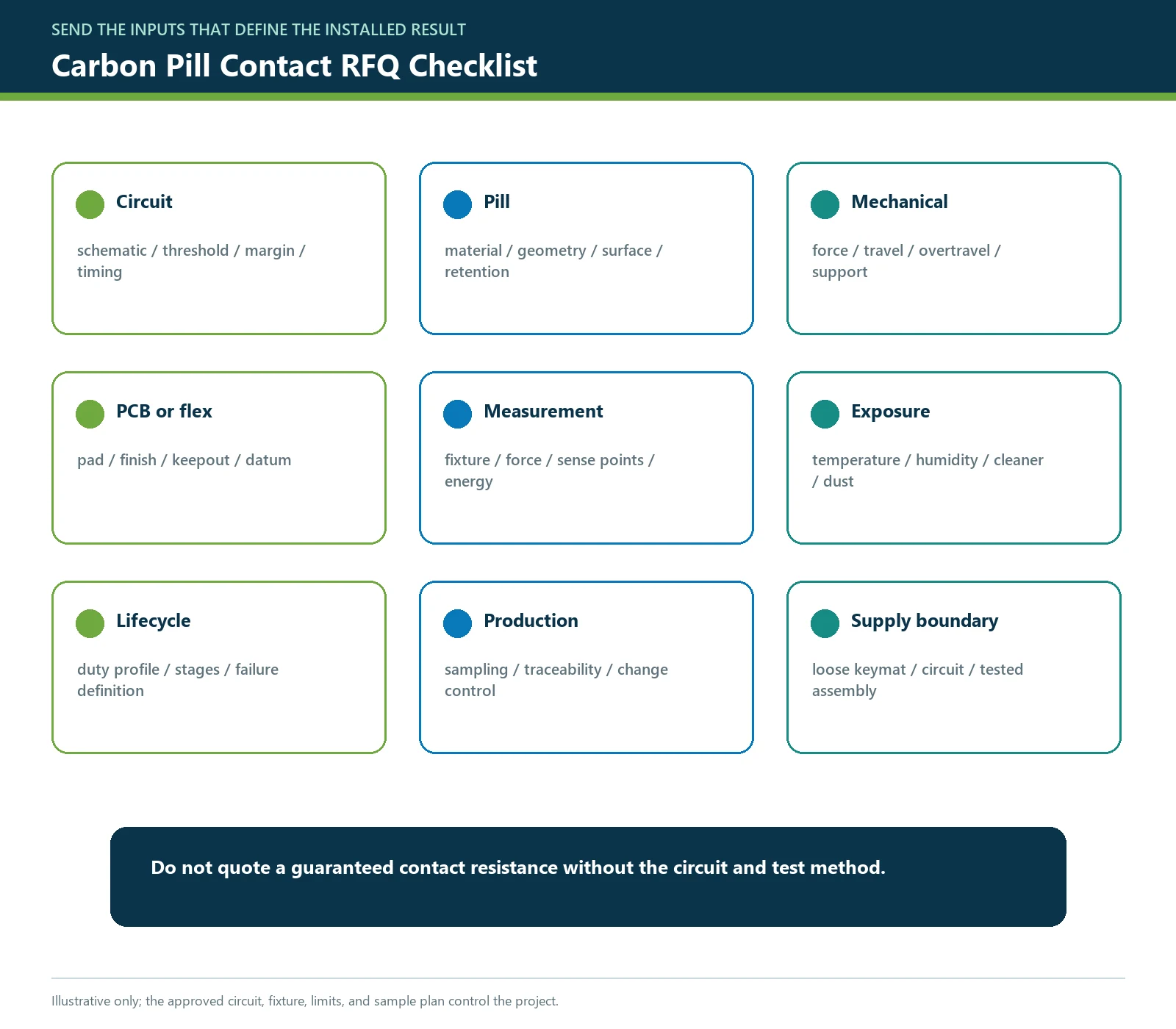
Carbon Pill Drawing and RFQ Checklist
Electrical
- input circuit and schematic;
- supply and threshold tolerances;
- pull-up/pull-down or matrix details;
- maximum total closed-path budget;
- allocated contact-resistance budget;
- open-state or leakage requirement;
- test voltage, current, polarity, timing, and sense points;
- low-level and functional test requirements;
- bounce/intermittency requirement; and
- powered lifecycle condition.
Pill and keypad
- pill material/grade or approved supplier route;
- pill outline, thickness, position, retention, and surface;
- key force-displacement curve;
- first touch, first closure, stable region, overtravel, and hard stop;
- center and edge press;
- key groups and high-use keys; and
- molding, cure, cavity, and change-control requirements.
PCB, FPC, or PET circuit
- pad artwork and dimensions;
- worst-case pill overlap;
- conductor and final contact surface;
- solder mask, via, trace, and component keepouts;
- local flatness and support;
- datum and locator scheme;
- cleaning, handling, storage, and packaging; and
- board/circuit supplier change control.
Validation and production
- initial, assembled, post-environment, and post-cycle limits;
- sample quantity, cavities, lots, and key selection;
- fixture drawing and calibration;
- raw waveform and summary-data retention;
- environmental and chemical exposures;
- cycle profile and inspection intervals;
- failure analysis and retest policy;
- production sampling or full test;
- supplied assembly boundary; and
- prototype and annual quantities.
Frequently Asked Questions
What resistance should a silicone keypad carbon pill have?
There is no universal value. Derive the maximum total closed-path resistance
from the product input threshold, pull-up/pull-down, supply, leakage, series
components, noise margin, temperature, and timing. Allocate only part of that
budget to the pill-to-pad contact, then validate it across force, samples,
environment, and life.
Is volume resistivity the same as contact resistance?
No. Volume resistivity is a normalized bulk-material property measured on a
defined specimen. Closed contact resistance includes two pill-to-pad interfaces,
the current path through the pill, pad geometry and finish, force, overlap,
contamination, and the selected measurement circuit.
Should contact resistance be measured with two wires or four wires?
Use two wires when total assembly-path resistance is the requirement and fixture
contribution is controlled and insignificant to the limit. Use four-wire sensing
when lead and fixture drops must be excluded. State the force and sense points in
either method.
Why can the measured resistance change with test voltage?
Surface films and non-ohmic interface behavior can make the result dependent on
measurement energy. A higher test voltage may disturb a film and report a lower
value. Separate low-level contact characterization from the actual product
functional test.
Does firmware debounce solve a high-resistance contact?
No. Debounce can ignore short transitions when voltage margin remains valid. It
cannot correct a closed path that never reaches the input threshold, stays
unstable, or develops long interruptions.
Should the carbon pill be tested before or after lifecycle cycling?
Both. Initial tests establish the release baseline. Periodic and final tests
show drift, intermittency, force changes, wear, contamination, and failure mode.
Use the production-intent circuit, support, load, environment, and electrical
condition.
Can a loose keypad pass while the installed keypad fails?
Yes. PCB flex, enclosure preload, support height, fastener sequence, alignment,
adhesive, spacer, and housing clearance can change contact force and overlap.
Compare loose and installed traces during validation.
What files are needed for a useful carbon-pill review?
Provide the keypad drawing/model, pill specification, PCB/FPC/PET contact
artwork, enclosure section, support and locator details, input schematic,
resistance budget, test method, force curve, environment, duty profile,
validation requirements, quantity, and launch timing.
Project Qualification Boundary
No material resistance, contact resistance, force, travel, current, voltage, life, temperature, humidity, chemical, pad, finish, or acceptance value is assigned to a JASPER project without a controlled drawing and approved test plan.
Request a Carbon Pill Contact Review
Send the input schematic, resistance budget, keypad and pill drawing, PCB
contact artwork, enclosure/support section, force curve, environment, duty
profile, and test expectations through the JASPER contact
page. Request a written response that
separates material control, contact geometry, measurement method, validation,
production test, and supplied assembly responsibility.
Ready to Start Your Project?
Tell us about your membrane switch, keypad, or graphic overlay requirements. Our engineering team will review your specifications and provide a detailed quote.