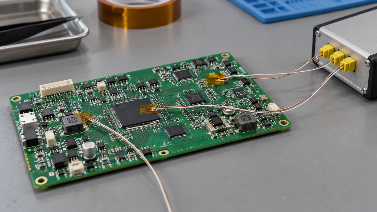
PCB assembly thermal balance means designing an assembly so its different regions can meet their soldering requirements without exceeding component or board limits. It does not mean equal copper coverage or identical temperatures everywhere. Review copper distribution, pad connections, component thermal mass, and exposure to oven heating together. Correct avoidable layout asymmetry, then hand a marked risk map to the process engineer. A copper-rich region is a candidate for slower heating, not a temperature measurement; its actual behavior depends on the assembled board and process.
- Identify Copper Imbalance and Mixed Thermal-Mass Regions
- Relate Pad Connections to Uneven Joint Heating
- Review Large Components Beside Thermally Sensitive Parts
- Compare Layout Mitigations Before Changing the Process
- Define Hot and Cold Locations for the Reflow Validation Handoff
- Record DFM Decisions and Remaining Thermal Risks
- Apply the Correct Specifications and Standards
- Apply the Review to Five Layout Scenarios
- 1. Power connector beside small passives
- 2. Exposed-pad power device on a copper-rich region
- 3. Dense region beside a sparse signal section
- 4. Depopulated product variant
- 5. Double-sided assembly in a production panel
- Next Step: Send a Thermal Risk Map with the Assembly Files
Identify Copper Imbalance and Mixed Thermal-Mass Regions
Copper imbalance matters when it changes the heat-storage and heat-transfer paths around joints. Review each copper layer and the populated assembly, not only the top-layer pour. Large components and large copper areas can heat more slowly during reflow. Treat that as a screening hypothesis rather than a rule that every plane-connected pad must be cold.
Separate three inputs: heat capacity, thermal connection, and exposure to heating. Heat capacity describes how much energy changes an object’s temperature. Connection geometry determines where heat can travel. Component height, placement, and assembly orientation affect exposure. A top-view copper image cannot resolve all three.
For a simple material comparison, heat capacity is approximately mass multiplied by specific heat. With identical material, footprint, and coverage, doubling actual copper thickness from 35 µm to 70 µm doubles that copper region’s heat-capacity contribution. It does not double the whole board’s heating time: laminate, components, heat transfer, and neighboring structures remain part of the system.
| Review variable | Options or measurement basis | DFM interpretation |
|---|---|---|
| Nominal starting copper thickness | 12 µm, 18 µm, 35 µm, 70 µm, 105 µm | These are documented starting-foil examples, not a universal catalogue or finished-copper guarantee. Obtain the finished stackup. |
| Copper coverage | A continuous percentage within a defined region, calculated separately for each layer | Compare equal-sized regions; record the inspection area and connected planes. Do not impose a universal balance percentage. |
| Pad connection geometry | Direct/solid connection; trace-neck connection; spoke thermal relief | Compare heat paths as well as electrical requirements. None is universally preferred. |
| Component thermal load | Material-dependent heat capacity in J/K; mass, construction, and dimensions as screening inputs | A large outline or high operating power alone does not quantify reflow response. |
Starting foil and finished copper are different specifications. Etching removes copper; plating can add copper. Use the fabrication stackup rather than assuming the nominal foil label describes every finished layer.
Likewise, package junction-to-ambient thermal resistance, usually expressed in °C/W, describes a defined operating heat-flow condition. It is not heat capacity in J/K. Do not use that number alone to rank transient reflow heating rates.
Relate Pad Connections to Uneven Joint Heating
Asymmetric pad connections can make neighboring joints wet at different times. Compare trace width, trace count, plane attachment, nearby plated holes, and via connections at both ends of a two-terminal component. The referenced supplier identifies these differences as contributors to unbalanced wetting and tombstoning.
Start with a paired-pad review. Trace each pad’s conductive path through every connected layer. Two surface lands can look identical while one connects through vias to a broad plane and the other reaches only a narrow trace. Equal land dimensions therefore do not establish equal thermal behavior.
A tombstoned or poorly wetted part is evidence of an assembly defect, not proof of a thermal root cause. Review paste deposits, placement, solderability, and the actual heating history before selecting a correction. Assembly quality reflects the combined effects of solder volume, board quality, placement and reflow conditions.
Where electrical constraints permit, compare more symmetrical trace entry, matched connection geometry, or a thermal-relief approach. Do not add spokes indiscriminately. For the PowerPAD thermal-via example, the specified heat-removal path uses continuous plane connections rather than thermal reliefs.
Treat a via’s solder-flow behavior and its conductive connection as separate questions. Closing a solder escape path does not demonstrate that both pads now have equivalent heat paths. Record both mechanisms when a design change addresses only one.
Review Large Components Beside Thermally Sensitive Parts
Large components beside thermally sensitive parts need a shared review because a setting that helps one location may challenge another. Examine the exact connector, shield, inductor, capacitor, or power package together with its smaller neighbors. Physical size is a screening cue; the component manufacturer’s assembly limits remain the controlling information.
Component placement can also affect access to heating. A tall connector or shield may alter local circulation around nearby parts; the importance depends on the heating system and geometry. Include layout, shadowing and tall-component proximity in the review of heat input.
Mark the potentially slow joint and the potentially limiting component separately. A connector’s solder terminals, plastic body, and nearby small passive do not necessarily represent the same temperature. Do not infer that the connector tolerates more exposure merely because it heats slowly.
Review the practical alternatives with the circuit designer: reposition the small part, rotate the connector, change the local arrangement, or select an assembly-compatible component. Preserve decoupling performance, signal integrity, mechanical fit, and current paths. “Move farther away” is not a complete instruction without those constraints.
Separate operating heat from assembly heat. A component that dissipates substantial power in service is not necessarily the slowest feature in an unpowered reflow assembly. Use its construction and connections to identify the concern, then use its assembly documentation to establish the relevant limitation.
Compare Layout Mitigations Before Changing the Process
For PCB assembly thermal balance, layout mitigation should come first when a local change removes an avoidable conflict without harming electrical function. Process adjustment remains appropriate when representative assemblies can satisfy all relevant limits together. Change the layout when necessary if hotter and colder locations cannot both fit the permitted process window.
Use the following matrix to convert design observations into review actions. Each risk is a hypothesis to investigate, not a predicted defect or a measured temperature classification.
| Design Feature | Thermal-Mass Effect | Potential Assembly Risk | Layout Option | Validation Handoff |
|---|---|---|---|---|
| Large copper plane | Adds distributed copper capacity and conductive paths; connected joints may lag | Inadequate joint exposure while other locations approach limits | Preserve necessary planes; review avoidable local asymmetry or component placement | Mark plane-connected joint groups, affected layers, and a contrasting region |
| Asymmetric pad connection | Couples opposite pads to different heat paths | Unequal wetting, component movement, or tombstoning | Compare trace entry and connection geometry; use relief only when permitted | Identify the paired pads and the exact geometric difference |
| High-mass connector | Metal terminals and housing construction add local load; body height can affect exposure | Late joint wetting or excessive exposure elsewhere | Reposition or rotate within mating constraints; review part selection | Supply connector limits and identify terminal versus body concerns |
| Dense power region | Concentrates copper, vias, and component loads | Narrow process margin between joint and component requirements | Review clustering and layer connections without compromising power return or cooling | Identify the region, retained electrical constraints, and limiting parts |
| Small part beside large mass | Small and large features can respond differently; local exposure may differ | Uneven wetting or excessive exposure of the smaller part | Reposition within circuit constraints; compare both pad connections | Mark the small part, neighboring mass, and the competing requirements |
| Uneven component distribution | Creates contrasting populated regions across the board or panel | Different thermal histories or unrepresentative sample selection | Review distribution, panel arrangement, and permitted orientation | State population variant, panel position, orientation, and assembly pass |
Do not add copper simply to make a coverage plot look symmetrical. Added copper can change electrical behavior and the heat-transfer network. Conversely, removing a necessary plane connection to simplify soldering can compromise the product’s operating requirements. Obtain electrical approval before accepting either approach.
When changing copper thickness or connection geometry, include fabrication feasibility in the decision. The referenced supplier notes that starting copper thickness affects achievable track and gap dimensions. A proposed neck or relief must therefore be checked against the selected fabrication rules, not copied from a different stackup.
The useful question is whether the proposed change removes the identified constraint. An oven adjustment that makes one problematic joint acceptable while pushing another component beyond its limit does not resolve the design conflict.
Define Hot and Cold Locations for the Reflow Validation Handoff
The thermal handoff should identify candidate regions and the reason each matters, while leaving final measurement locations and the process window to the validation engineer. Distinguish a candidate slow-heating joint, a candidate high-exposure component, and an asymmetric pad pair. These are different review objects, even when they occupy the same neighborhood.
Annotate assembly views with reference designators, board side, region boundaries, and links to the affected copper layers. Include both dense and sparse regions rather than selecting only the largest component. Specify whether the concern is solder-joint exposure, component-body exposure, or a mismatch between adjacent joints.
Actual component temperatures depend on location and surrounding population; oven settings do not directly represent solder-joint temperatures. This is why the marked layout is an input to validation rather than a replacement for it.
| Handoff item | Information to provide | Decision it supports |
|---|---|---|
| Controlled build identity | Board revision, BOM variant, assembly side, panel drawing, and assembly sequence | Whether the tested build represents the released product |
| Copper and connection evidence | Layer stackup, finished-copper requirement, plane connectivity, relevant vias, and paired-pad views | Whether the suspected thermal difference exists in the actual design |
| Competing limits | Exact component assembly documents, solder-paste guidance, board requirements, and applicable exposure history | Which joint and material constraints must be satisfied together |
| Representative process conditions | Intended orientation, panel or carrier configuration, loading condition, and reflow pass | Which changes could make previous evidence unrepresentative |
| Risk closure evidence | Correlated temperature records, inspection results, accepted design revision, and responsible reviewers | Whether the layout concern has been demonstrated acceptable |
The process engineer should decide the final sensor locations, attachment methods, instrument suitability, and acceptance window. This handoff does not prescribe a universal temperature difference, peak temperature, or oven recipe.
Before treating a previous trial as applicable, compare its stackup, population, panel configuration, and assembly sequence with the proposed build. A useful report connects the measured locations back to the risk map and explains how the selected conditions represent the intended production build.
Every flagged concern needs a disposition, but not necessarily its own measurement point. The process engineer can justify representative coverage where regions are equivalent. Require that rationale to identify the shared construction and limiting conditions; a convenient sensor location alone does not establish equivalence.
Record DFM Decisions and Remaining Thermal Risks
A thermal DFM decision should state what changed, what constraint was retained, who accepts the tradeoff, and what evidence closes the concern. A design-rule check confirms geometry against its configured rules; it does not prove a soldering window exists. Keep the design decision connected to its validation requirement.
Consider an illustrative Rev C controller, risk TB-03, not a production test result: R17 sits beside connector J2, with one pad tied directly to a ground region and the other connected by a narrow trace. The proposed disposition is to evaluate matched trace-neck connections without cutting the required ground plane. Electrical design owns current and return-path approval; layout owns the revised paired-pad view; manufacturing owns representative thermal validation; quality owns review of the linked inspection evidence. Release requires the accepted geometry and supporting evidence to refer to the same controlled revision.
That record is more useful than “optimize profile” because it names the affected item, preserves the electrical constraint, and defines closure. An unchanged design also needs a reason: for example, the required current path prevents a relief change, so acceptance depends on documented validation of that retained geometry.
Record triggers for renewed review, including a copper-stack change, connector substitution, population change, or altered panel configuration. Do not automatically carry a thermal decision into a materially different build.
Apply the Correct Specifications and Standards
The applicable thermal constraints come from the actual component, board, and assembly process. Read the component’s assembly guidance, the solder-paste supplier’s requirements, and the agreed bare-board specification together. A generic profile diagram is not a substitute for that document set.
J-STD-020 concerns moisture/reflow sensitivity classification of applicable nonhermetic surface-mount devices. A classification exposure is not automatically the board’s production recipe. Distinguish solder-joint requirements from component-body limits; retain that distinction when translating documents into validation criteria.
Package-specific layout guidance also takes precedence over a generic suggestion to weaken thermal connections. Preserve required exposed-pad and via connections unless the responsible designer approves a supported alternative.
Keep temperature evidence and joint-quality evidence separate. An acceptable thermal record does not, by itself, demonstrate every joint’s workmanship. Equally, an acceptable-looking sample does not establish temperature margin across the build. Agree the inspection approach and product acceptance requirements alongside validation, including appropriate evaluation of joints hidden beneath packages.
Apply the Review to Five Layout Scenarios
The following scenarios show how the same review changes with the assembly. They are representative design situations, not reported JASPER production results. Each requires a different risk map rather than a different universal recipe.
1. Power connector beside small passives
Flag the connector terminals and the nearby passive pad pairs separately. Check whether a passive’s plane connection compounds the local difference. Evaluate repositioning within circuit and mating constraints before asking the process engineer to increase overall exposure. Carry the exact connector’s body limits into the handoff.
2. Exposed-pad power device on a copper-rich region
Preserve the package’s required operating heat-removal path. Investigate the solder-joint concern without automatically adding thermal relief to the thermal-via network. Mark the region and its neighboring limiting components so validation addresses both the required joints and the surrounding assembly.
3. Dense region beside a sparse signal section
Compare the two regions using the same board revision and stackup. Identify the joint group that may lag and the part whose permitted exposure may constrain adjustment. Avoid treating a board-average temperature as evidence that both regions satisfy their individual requirements.
4. Depopulated product variant
A variant that removes a connector, shield, or component bank changes the population used in the review. Compare the revised load and exposure pattern with the validated configuration. Document the equivalence rationale or identify the additional validation needed; do not assume the less-populated version is automatically easier.
5. Double-sided assembly in a production panel
State which side and which assembly pass the risk map covers. Include panel rails, carriers, and orientation where they affect the intended build. Identify previously assembled components whose exposure limits remain relevant. Keep this thermal review separate from decisions about support, transport, and board deformation.
Frequently Asked Questions
How can copper balance affect reflow assembly?
Copper distribution changes heat storage and heat transfer around solder joints. Broad planes, thicker copper, and multilayer connections can create different responses across an assembly. Review them with component population and heating conditions, then validate the identified regions. Equal copper coverage alone does not establish a suitable reflow process.
Why can neighboring pads heat at different rates?
Neighboring pads can connect to different amounts of copper through traces, planes, and vias. That changes their heat paths even when their surface dimensions match. Uneven exposure can contribute as well. Investigate paste, placement, and solderability alongside heating evidence before assigning a defect to thermal asymmetry.
Can a single oven recipe compensate for every thermal-mass difference?
No single oven recipe can be assumed to accommodate every thermal-mass difference. The relevant question is whether a representative assembly satisfies solder-joint requirements without exceeding component and board limits. Where those requirements conflict, layout or component changes may be necessary rather than further process adjustment alone.
Which layout areas should be flagged for temperature-profile validation?
Flag copper-rich joint groups, asymmetric pad pairs, large connectors, dense power regions, small parts beside large masses, and contrasting population areas. Identify the specific concern at each location and include relevant variants and assembly passes. The validation engineer then selects the final measurement locations and acceptance criteria.
When should a thermal assembly risk be fixed in layout rather than by process tuning?
Fix the risk in layout when an avoidable connection or placement difference can be removed without compromising electrical function, or when the assembly cannot meet its competing thermal requirements together. Use process tuning where representative validation demonstrates compatibility. Close the decision with linked design, temperature, and inspection evidence.
Are thermal reliefs always the right correction?
Thermal reliefs are not always appropriate because some connections must carry current or conduct operating heat into a plane. Package guidance may require continuous connections at thermal vias. Compare the proposed relief with the actual electrical, thermal, and fabrication requirements before accepting it as a soldering improvement.
Does thicker copper automatically improve assembly thermal balance?
Thicker copper does not automatically improve assembly thermal balance. It changes local heat capacity and conduction, while the rest of the board and the heating process still influence temperature response. Specify actual finished-copper requirements and review the distribution across layers instead of selecting thickness solely to equalize reflow heating.
What should be included in a thermal DFM handoff?
Include the controlled assembly revision, population variant, layer stackup, marked risk regions, relevant pad connections, component limits, and intended panel and process conditions. Identify the responsible reviewers and closure evidence. Leave final measurement placement and the validated reflow window to the process engineer rather than prescribing them from layout alone.
Next Step: Send a Thermal Risk Map with the Assembly Files
A useful thermal review starts with the design evidence, not a request for a standard oven setting. Prepare the fabrication and assembly data, stackup, BOM with exact part numbers, placement information, and panel configuration. Add annotated regions that explain the suspected imbalance and the electrical constraints that cannot be changed.
Send that package to JASPER when discussing PCB assembly services. Ask which concerns require a layout decision and which require process validation. The desired outcome is a traceable decision for each thermal risk, with clear responsibility for demonstrating that the intended assembly meets its requirements.
Ready to Start Your Project?
Tell us about your membrane switch, keypad, or graphic overlay requirements. Our engineering team will review your specifications and provide a detailed quote.