
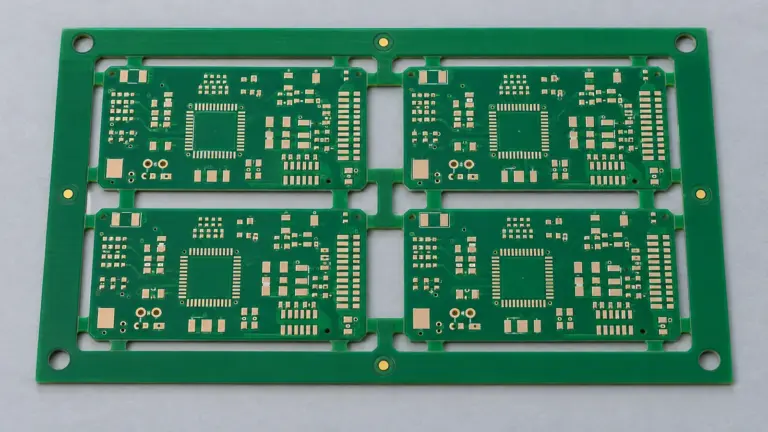
PCB Fiducials: Global and Local Alignment
Review PCB assembly fiducials with board and panel diagrams, local alignment checks, mask-clearance guidance and process-specific design reference examples.
Read the engineering note →Engineering notes for membrane switch drawings, sample approval, RFQ preparation, and tooling review before production starts.
Review PCB assembly fiducials with board and panel diagrams, local alignment checks, mask-clearance guidance and process-specific design reference examples.
Read the engineering note →
Review PCB panelization for assembly with rail, fiducial, support and separation checks. Approve panel drawings around real line and fixture requirements.
Read the engineering note →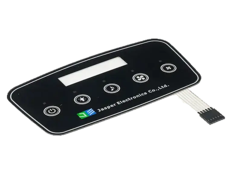
Compare capacitive sliders, wheels and buttons for custom control panels. Define mapping, endpoints, wraparound, feedback and prototype acceptance tests.
Read the engineering note →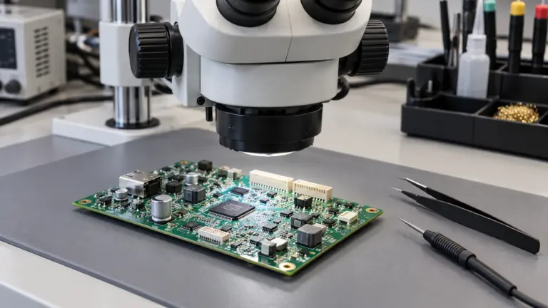
Review PCB assembly component clearance for placement, inspection, rework, connector mating, fixtures, and final integration with package and tooling evidence.
Read the engineering note →
Compare capacitive coupling, metal-over-cap and inductive touch for metal-front controls. Define force, panel motion, wet-use tests and supplier responsibilities.
Read the engineering note →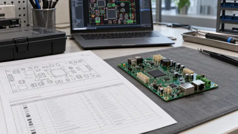
Use this PCB assembly DFM checklist to review footprints, panel handling, soldering, inspection and rework, then close release-blocking issues with evidence.
Read the engineering note →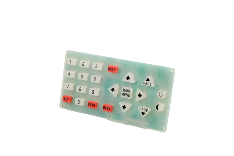
Compare off-the-shelf and custom silicone keypads by fit, graphics, tooling, integration cost, revision control and prototype risk for OEM equipment.
Read the engineering note →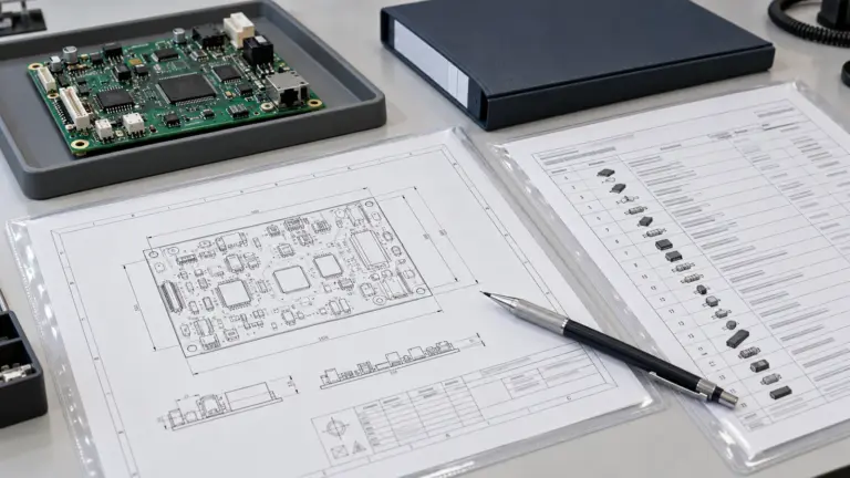
Build a PCBA manufacturing release package that controls BOM, firmware and test changes, defines batch effectivity, and records approvals and supplier handoff.
Read the engineering note →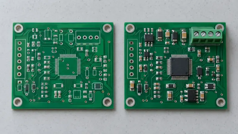
Manage PCB assembly BOM variants by linking each board revision to fitted parts, firmware, configuration, labels and tests before releasing an OEM build.
Read the engineering note →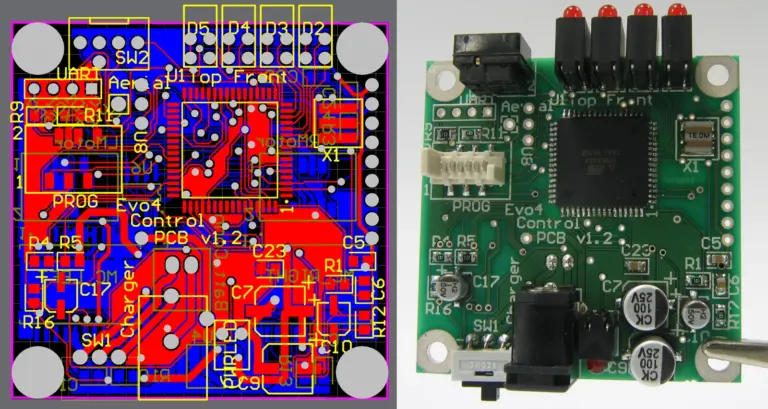
Compare Gerber, ODB++ and IPC-2581 for PCB assembly. Check BOM and placement coverage, importer compatibility, data loss and release authority before handoff.
Read the engineering note →
Resolve PCB assembly polarity and pin 1 conflicts with a practical checklist for component markings, footprint mapping, engineering approval and repeat builds.
Read the engineering note →
Control DNP and DNI PCB assembly with consistent BOMs, placement files, drawings, inspection rules, and test settings for approved unpopulated positions.
Read the engineering note →