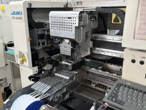
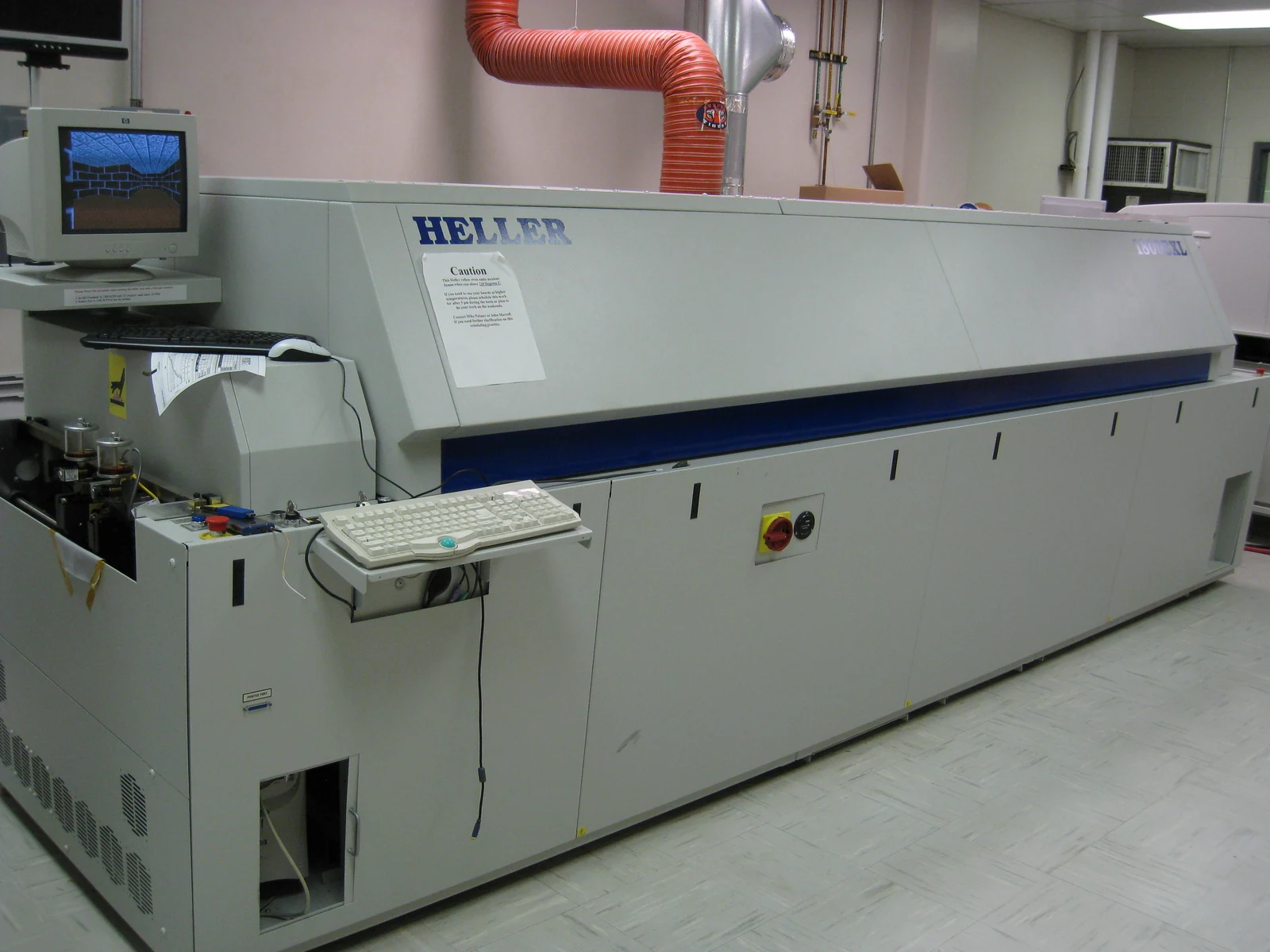
Single-sided PCB assembly places components on one board face; double-sided assembly uses both faces, regardless of copper layer count. Choose one populated side when the circuit fits with suitable routing, cooling and access. Add the second side when a smaller footprint or necessary component location justifies the extra operations. For conventional sequential SMT, budget for 2 reflow passes and check first-side components for both thermal exposures. The cost difference comes from printing, handling, support and verification, not a universal multiplier.
Photo: Nelatan / Wikimedia Commons · CC BY-SA 3.0.
- Single-Sided vs Double-Sided PCB Assembly at a Glance
- Assembly Sides Are Not the Same as Copper Layers
- Placement Density and Access on One or Two Sides
- Second-Side Reflow and Component-Retention Questions
- Heat exposure and profile limits
- Retention during the second pass
- Stencils, Fixtures and Handling Between Passes
- Inspection, Rework and Keepout Constraints
- Where Single-Sided Assembly Wins
- Production Process
- Product Geometry
- Service and Verification
- Where Double-Sided Assembly Wins
- Production Process
- Product Geometry
- Service and Verification
- When Double-Sided Assembly Justifies the Added Operations
- Compare the quote on equal terms
- Final Recommendation
Single-Sided vs Double-Sided PCB Assembly at a Glance
Single-sided assembly is the simpler production choice when both layouts meet the product requirements. Double-sided assembly earns its place when using the underside solves a real packaging or placement problem. Compare feasible layouts with the same BOM, test coverage and order quantity before choosing.
| Project priority | Preferred starting point | Reason to change the choice |
|---|---|---|
| Lowest assembly effort with adequate board area | Single-sided assembly | The larger board increases enclosure or fabrication cost enough to outweigh the added assembly work |
| Fixed, crowded board outline | Double-sided assembly | Underside height, support or test access prevents usable placement |
| Direct access for repair and probing | Single-sided assembly | A two-sided layout still preserves the required tool and probe access |
| Components needed on opposite product faces | Double-sided assembly | A connector or mechanical redesign removes that requirement at lower total cost |
A second assembly face creates placement space. It does not automatically improve electrical performance, increase reliability or reduce the required copper layers.
Assembly Sides Are Not the Same as Copper Layers
Assembly sides describe where component bodies are mounted; copper layers describe the PCB’s conductive stack-up. A multilayer PCB can have all its components on one face. A board with two copper layers can also use either one or both faces for components. Through-hole leads soldered on the reverse face do not, by themselves, create a second component mounting side.
The two assembly options are 1 populated side and 2 populated sides. For a conventional all-SMT route, their usual production sequences are 1 reflow pass and 2 reflow passes, respectively. Extra selective soldering, manual operations or rework must be counted separately.
Use the following comparison with the BOM, bare-board specification, quantity and acceptance requirements held constant. Changes to board size or the enclosure belong in a separate product-cost comparison.
| Assembly Factor | Single-Sided Build | Double-Sided Build | Cost Mechanism | Design Check |
|---|---|---|---|---|
| Component placement | One populated face and its placement program | Two populated faces and side-specific placement data | Second setup, alignment and board transfer; total placement count need not increase | Confirm centroid side, rotation, polarity and do-not-fit positions |
| Reflow sequence | Normally one production reflow for an all-SMT build | Normally sequential reflow of the first and second sides | Another oven operation, handling and profile verification | Check first-side parts for two exposures and inverted retention |
| Stencil preparation | One side-specific paste pattern | Two side-specific paste patterns | Paste tooling, setup, print inspection and cleaning; physical stencil count depends on tooling strategy | Review aperture geometry and paste volume for each side |
| Board support | Unpopulated reverse face offers more support locations | Existing underside parts restrict supports and carriers | Support programming, dedicated tooling where needed and loading time | Check package heights, rails, panel stiffness and support contact locations |
| Inspection access | One component face to inspect, plus relevant solder-side features | Inspection access and coverage for both faces | Extra orientation, inspection programming and review | Preserve optical sightlines, hidden-joint inspection and test access |
| Rework exposure | Opposite face usually has fewer component obstructions | Opposite-side parts may obstruct tools or receive unwanted heat | More setup, shielding, support and verification after repair | Check nozzle clearance, local heating and remaining component thermal allowance |
The procurement specification should state both the copper stack-up and the populated sides. “Double-sided PCB” alone is ambiguous in an assembly RFQ.
Placement Density and Access on One or Two Sides
Double-sided assembly adds placement area, but the board outline is a poor measure of usable underside space. Mounting hardware, enclosure ribs, connector insertion paths, supports and test probes compete with the new footprints. Check the assembled geometry.
Start with the mechanical model and reserve the height available above and below the PCB, including the space needed to insert connectors, support the panel during printing and reach components during service. An apparently empty underside region may sit directly over a chassis boss. That space is already taken.
Moving decoupling components under an IC can shorten connections in a suitable layout. The benefit depends on the actual via and return-path arrangement; relocating a component to the opposite face does not, by itself, produce a better electrical design.
Placement count is a separate question. For an illustrative BOM with 120 SMT placements, moving 24 underneath leaves 96 on the first face and 24 on the second: the total remains 120. What changes is the route. Request separate pricing for the second setup, board transfer and support arrangement so that these charges are not confused with an increase in component quantity.
Second-Side Reflow and Component-Retention Questions
Sequential double-sided reflow heats the PCB twice. Components fitted first must therefore tolerate a second exposure while facing downward, whereas components added for the second pass normally receive one production reflow exposure. Use two first-side exposures as the design-review benchmark. Assess repair heating separately.
A conventional sequence is:
Single-sided SMT:
Print paste → inspect paste → place components → reflow → inspect → electrical test

Double-sided SMT:
Print first side → inspect paste → place first side → reflow → inspect
→ flip and support board → print second side → inspect paste → place second side
→ reflow → inspect both faces as specified → electrical test
The drawing does not choose the order. “First side” can mean the CAD top or bottom face, depending on which sequence accommodates the packages, supports the next print and leaves the required inspection access.
Heat exposure and profile limits
Check actual package recommendations for allowable cycles, peak body temperature, time at temperature and moisture handling, then verify that the coldest joint receives enough heat to solder without taking the hottest package beyond its limits. Validate both board orientations with their production supports. NXP AN10365 explains this process window and the moisture-control implications of the interval between passes.
A classification profile is not an oven recipe. Infineon’s dual-row gullwing guidance describes three qualification reflow runs for its relevant MSL-classified components, representing double-sided assembly and a rework cycle. Apply that example only within its package scope. Infineon’s assembly recommendations also identify top-side-cooled packages that should avoid inverted second reflow because joint stand-off can change.
Retention during the second pass
First-side solder can melt again. An inverted component’s retention depends on its mass, pad geometry, solder wetting and process conditions; a small body may stay attached, but size alone cannot establish that it will survive the actual profile and board transport. Texas Instruments’ power-module guidance evaluates component and pad characteristics and discusses supporting fixtures.
Assemble heavier parts second where feasible. This often avoids an inverted reflow for those parts, although the first-side packages still need review. If the sequence cannot be changed, consider a qualified retention method or a different installation operation. Adhesive adds its own dispense, cure and repair requirements. It is not a default requirement for every double-sided board.
Stencils, Fixtures and Handling Between Passes
Double-sided SMT adds a paste-printing operation and requires support around parts already fitted underneath. Review print support and reflow retention separately. A support that keeps the PCB flat under the squeegee may do nothing to restrain an inverted component when its solder melts.
Each face needs its own paste pattern. Two patterns do not always require two separately framed stencils: a suitable combined tool or panel arrangement can carry both, provided the printer setup, alignment and clearance work for the actual build. Define the supplied tooling, its ownership and the changes that trigger replacement.
Paste volume matters. Select stencil thickness and apertures for the package mix on each face, especially where a fine-pitch IC shares that face with a connector requiring more solder. Copying the first-side stencil specification can leave the second-side packages with unsuitable deposits.
Check the full support path, from paste printing through placement, transfer and reflow, against the panel outline and underside component heights. Supports must avoid vulnerable parts while holding the board sufficiently stable for the operation. Include rails and breakaway areas in that review.
The interval between passes also needs control. Protect exposed components from impact and ESD, and track moisture-sensitive devices through storage and the next heating step. A queue can change the handling requirements. It does not change the BOM.
Inspection, Rework and Keepout Constraints
Double-sided assembly needs an inspection and repair plan for both component faces. Reserve the necessary access before releasing the layout. A circuit can be electrically correct yet costly to verify once underside components occupy the places intended for probes, supports or repair tools.
Solder Paste Inspection (SPI) checks deposits before placement, while Automated Optical Inspection (AOI) assesses visible features within its programmed coverage. BGA and other hidden-joint packages may need specified X-ray inspection. AOI cannot see through a package. Opposing components can also complicate the interpretation of X-ray images.
Define electrical coverage separately. In-Circuit Test (ICT), flying-probe tests and programming connections need reachable nodes, compatible support and agreed limits; simply adding an inspection view of the reverse face does not establish that the assembled circuit works.
Repair adds another access problem. During removal or replacement of a component, heat can reach an opposing package even when that package is outside the immediate work area, so the rework plan must consider reverse-side devices as well as the target joint. Check nozzle clearance, local support and cumulative thermal exposure. Specify the checks after repair.
Keepouts must cover placement, support, probing and repair, together with the installed enclosure. The tool determines the clearance. Use actual tool geometry and package restrictions instead of treating one spacing number as sufficient for every operation.
Where Single-Sided Assembly Wins
Single-sided assembly wins when a practical one-face layout meets the electrical, mechanical and test requirements. Fewer side-dependent operations and fewer underside obstructions make it a useful baseline. Keep that baseline unless the second face delivers a product benefit.
Production Process
One populated face avoids the second paste-printing and placement sequence in a conventional all-SMT build. The production team also avoids qualifying inverted retention for a second reflow, although any later soldering or repair operation still needs its own thermal review. This can simplify prototype changes. Material supply still affects delivery.
Product Geometry
Consider an illustrative 80 mm × 60 mm control board that already fits its enclosure with the required routing and cooling. Its 4,800 mm² outline area need not shrink simply because components could move underneath. Preserving the clear reverse face may provide more value through mounting supports, a thermal interface or a restricted enclosure gap.
Service and Verification
One populated face can leave a more direct route for probes and replacement tools. Access still requires design work. Preserve reachable nodes and stable support, then choose single-sided assembly when those practical service benefits outweigh the value of recovering underside placement area.
Where Double-Sided Assembly Wins
Double-sided assembly wins when the second populated face resolves a meaningful space or component-location constraint. Confirm the resulting production route. A smaller outline only helps if the assembled board still has sufficient clearance, thermal margin and access for verification.
Production Process
For a stable design, repeat production can distribute one-time tooling and programming charges over more units. The second-side operations remain recurring costs, so compare actual batch sizes and setup assumptions before deciding that volume makes the two-sided route economical. Tooling reuse needs agreement.
Product Geometry
In the same illustrative layout study, assume a feasible two-sided design reduces the 80 mm × 60 mm outline to 60 mm × 60 mm. Area falls from 4,800 mm² to 3,600 mm², a 25% reduction. That can solve an enclosure constraint. It does not establish a 25% fabrication saving, because panel utilization and the quoted process still determine cost.
Service and Verification
Two-sided placement can reserve a useful region for connectors or servicing while moving other parts elsewhere. Keep the probes reachable. The option wins when this allocation preserves inspection and repair access; occupying every underside footprint would defeat that purpose.
When Double-Sided Assembly Justifies the Added Operations
Double-sided assembly justifies its extra operations when the verified product benefit exceeds the incremental manufacturing cost and the route meets the project’s thermal, support and access requirements. Compare feasible designs first. A price advantage cannot make an obstructed test point or an unsuitable package reflow-compatible.
| Project constraint | Choose or investigate | Release condition |
|---|---|---|
| Components fit comfortably on one face | Single-sided assembly | Routing, cooling and test access meet the product requirements |
| A fixed outline cannot accommodate the parts on one face | Double-sided assembly | The mechanical model provides usable underside height and support access |
| Heavy or top-side-cooled packages dominate one face | Assemble that face second where feasible | Package restrictions and retention of the first-side components are satisfied |
| First-side parts have limited thermal tolerance | Reorder, change parts or revise the route | Each first-side part supports the planned two production reflow exposures within its own limits |
| Underside components obstruct required probes or repair tools | Revise placement before adding the second face | Fixture, programming and rework access are demonstrated on the proposed layout |
| Tooling cost dominates a small order | Compare one-sided and two-sided quotations | Separate one-time engineering/tooling from recurring setup and unit costs |
Compare the quote on equal terms
Separate the assembly premium from the product saving. A smaller outline can change panel utilization and bare-board pricing, while adding components to the reverse face without altering the board specification does not itself change the copper stack-up or establish a fabrication saving.
Use this comparison:
Incremental delivered cost per board = added per-board operations + added batch setup / batch quantity + incremental one-time tooling / agreed amortization quantity − verified product savings per board.
Keep the currency and delivery scope consistent. Use the actual batch quantity for repeat setup, and state the quantity over which one-time costs are distributed so that a prototype order is not compared with an assumed lifetime production run. Include yield or repair allowances on an agreed, defensible basis. This is a calculation framework, not a quotation.
| Review item | OEM input | Assembler response | Purchasing check |
|---|---|---|---|
| Placement and sequence | BOM, side-tagged centroid data, assembly drawings | Proposed side order and exceptions | Same fitted parts and revision in both quotes |
| Tooling and support | Panel outline, component heights, mechanical restrictions | Paste tooling, supports, carriers and their revision needs | Identify one-time charges, ownership and reuse |
| Verification and repair | Required inspection, test coverage and service constraints | Inspection orientations, test access and repair approach | Same acceptance scope and defined exclusions |
| Order basis | Prototype quantity, repeat-batch quantity and expected changes | Setup, recurring operation and tooling costs | Separate batch charges from per-board charges |
Settle responsibility before release. The OEM supplies the design restrictions and acceptance needs; the assembler proposes a workable sequence and the corresponding tooling and inspection scope; purchasing compares those agreed assumptions in the quotations. An undefined second-side inspection plan leaves the offers on different terms.
Frequently Asked Questions
Single-sided and double-sided PCB assembly differ in populated faces and the operations needed to build them. The following answers connect those choices to the board stack-up, soldering sequence and quotation.
Can a multilayer PCB have components on only one side?
Yes. Copper layer count and component mounting sides are separate design choices. A multilayer board with components on one face is a single-sided assembly, even though internal layers provide routing, power and ground connections.
Does double-sided assembly always require two reflow passes?
No. Two reflow passes are the normal baseline for conventional sequential SMT on both faces. A mixed-technology or manually completed build can use a different combination of reflow, selective, wave or hand soldering. Specify the actual route rather than deriving every operation from the number of populated sides.
What determines which board side is assembled first?
Component retention, thermal limits, support access and the inspection plan determine the first side. Heavier or otherwise restricted packages often belong on the second side. Check first-side parts for two production reflow exposures and inverted processing; CAD top and bottom labels do not establish manufacturing order.
Can heavy components be mounted on the second side?
Yes, when their package limits and the production route allow it. Mounting heavy components during the second pass often avoids an inverted reflow for those parts. Final-use vibration and mechanical loading still need their own mounting assessment, separate from solder retention inside the oven.
Which quote items change when a board becomes double-sided?
Paste tooling, side-specific programming, setup, printing, handling, support and inspection can change. The route may also need retention tooling or a different repair approach. Separate one-time charges from recurring costs, and compare the same BOM, quantity, board specification and test coverage.
Does double-sided assembly cost twice as much?
No fixed multiplier applies. The second side adds operations, but moving components between faces does not double the component count or material cost. Total economics also depend on tooling, batch size, test access and any verified board or enclosure savings.
Does double-sided assembly need two separate stencils?
It needs two side-specific paste patterns for the conventional printed-paste SMT route, but not necessarily two separately framed stencils. Panel design and tooling strategy determine the physical stencil arrangement. The quote should identify what is supplied and what can be reused.
Is double-sided assembly less reliable than single-sided assembly?
Double-sided assembly is not inherently less reliable. Reliability depends on the design, materials, qualified process and operating conditions. Extra thermal exposure, inverted retention and repair access require attention, but side count alone cannot establish a reliability rating.
Final Recommendation
Choose single-sided assembly when one populated face meets the product’s requirements with suitable access. Choose double-sided assembly when the second face delivers a clear packaging or placement benefit and its added operations have been reviewed and priced.
Prepare the BOM, side-tagged placement files, assembly drawings, mechanical model, quantities and required test coverage. Mark components with special reflow or retention restrictions, and request the proposed assembly order plus separate tooling and recurring charges.
For a JASPER project, use the PCB assembly services enquiry route to discuss that package and the one-sided or two-sided build options. Settle the side sequence, support approach and acceptance scope before releasing the layout for production.
Ready to Start Your Project?
Tell us about your membrane switch, keypad, or graphic overlay requirements. Our engineering team will review your specifications and provide a detailed quote.