
OEM silicone keypad engineering resource
Silicone Rubber Keypad Design Guide for OEM Products
A silicone rubber keypad should be designed as a force path from the operator to the circuit, not as a molded cover added after the PCB is finished. Release the key shape, web, compound, travel, contact, circuit support, legends, lighting, enclosure compression, tooling inputs, and acceptance evidence as one installed system.
JASPER’s custom silicone rubber keypads can be reviewed as a loose molded keymat or as part of a stack with conductive contacts, PCB/FPC/PET circuit, LEDs, connector, spacer, adhesive, and enclosure features. The quotation should identify the supplied boundary, the customer-owned parts, the force and electrical acceptance method, and the assembly that represents production use.
What Is a Silicone Rubber Keypad?
A silicone rubber keypad is a molded elastomer part with one or more raised keys that deform under finger load and return when the load is removed. The molded key may carry a conductive contact, actuate a metal dome or mechanical switch, or transfer force to another circuit element.
The rubber does two jobs at once:
- it creates the visible and tactile user surface; and
- it acts as a spring, guide, seal component, light-control feature, or assembly interface.
That combination is why a keypad cannot be fully specified by outside dimensions and color. A key that looks correct can still wobble, bind, actuate too early, miss the contact pad, leak light, rub a coating, or change feel after installation.
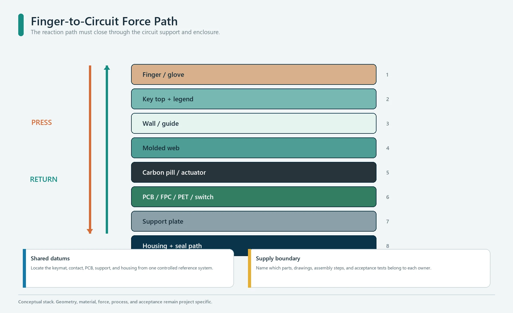
Draw the Finger-to-Circuit Stack
Start with a section through one representative key:
finger or glove
      |
key top, legend, texture and coating
      |
key wall, guide feature and molded web
      |
carbon pill, actuator or other contact element
      |
PCB, FPC, PET circuit, membrane layer or discrete switch
      |
support plate, housing ribs, bosses and fasteners
      |
enclosure seal path and product structure
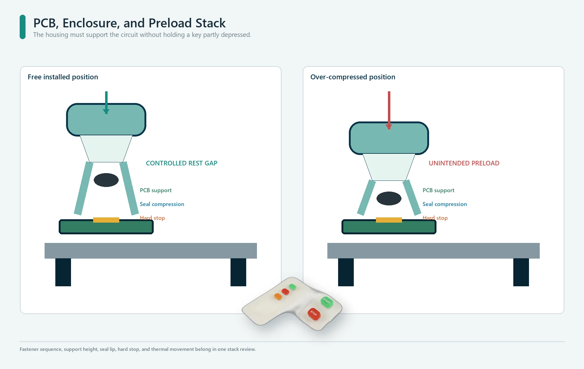
The force path must close through the support structure. If the PCB flexes, the housing pocket is too deep, a gasket remains over-compressed, or the keypad is not positively located, the installed key response can differ from the bench sample.
Name the responsibility at every interface
For each boundary, record:
- who supplies the part;
- which drawing controls the interface;
- which datum locates it;
- which test approves it; and
- who owns a change after sample approval.
This prevents the keypad supplier, PCB supplier, and enclosure molder from each assuming that another party controlled the same stack height.
Select the Switching Architecture Before Tuning Feel
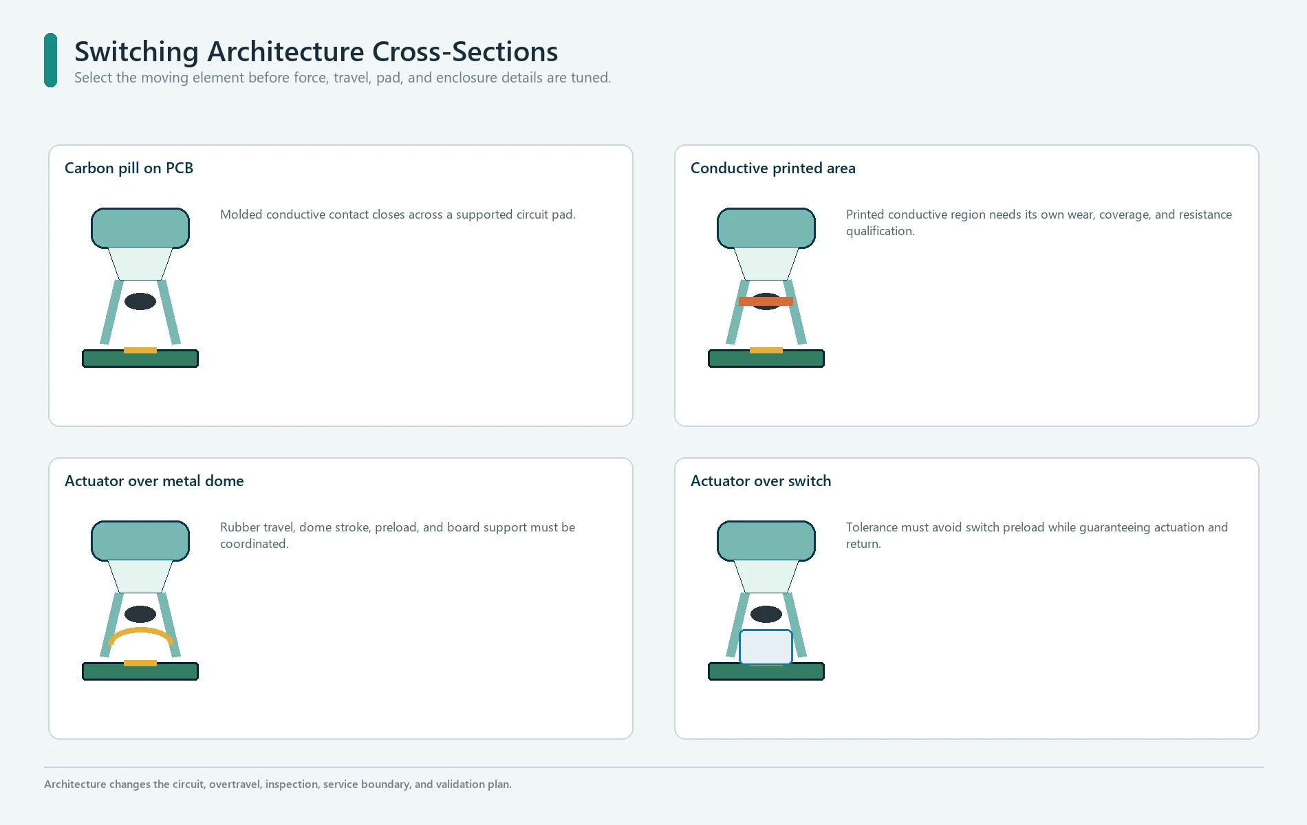
The same molded silicone surface can operate several electrical structures.
| Architecture | What moves under the key | Main design question | Suitable project direction |
|---|---|---|---|
| Conductive carbon pill | A molded-in conductive pill lands across PCB or circuit pads | Does the pill overlap the pad and close before harsh bottoming? | Integrated rubber contact with a simple circuit interface |
| Conductive printed area | A conductive region on the rubber contacts the circuit | Can print coverage, wear, resistance, and location be controlled? | Custom contact shape that has been specifically qualified |
| Silicone actuator over metal dome | The rubber presses a separate tactile dome | Are rubber travel, dome stroke, preload, and support coordinated? | Crisp dome feedback behind a molded key surface |
| Silicone actuator over mechanical switch | A molded post presses a board-mounted switch | Does the tolerance stack avoid preload and guarantee actuation? | Electronics already use discrete switches |
| Non-contact or light-only key feature | The rubber supplies the surface, light path, seal, or guide | Which separate sensor or switch owns the electrical function? | Special HMI stack with another input technology |
Do not choose the contact method only from resistance or unit cost. It changes the PCB pattern, actuation sequence, overtravel, contamination risk, inspection, service boundary, and life test.
For projects centered on a molded-in conductive contact, the conductive rubber keypad page defines the commercial route. Detailed carbon-pill resistance and PCB contact qualification belong in a separate electrical-contact study, not in a generic keypad drawing.
Define Key Feel with a Force-Displacement Curve
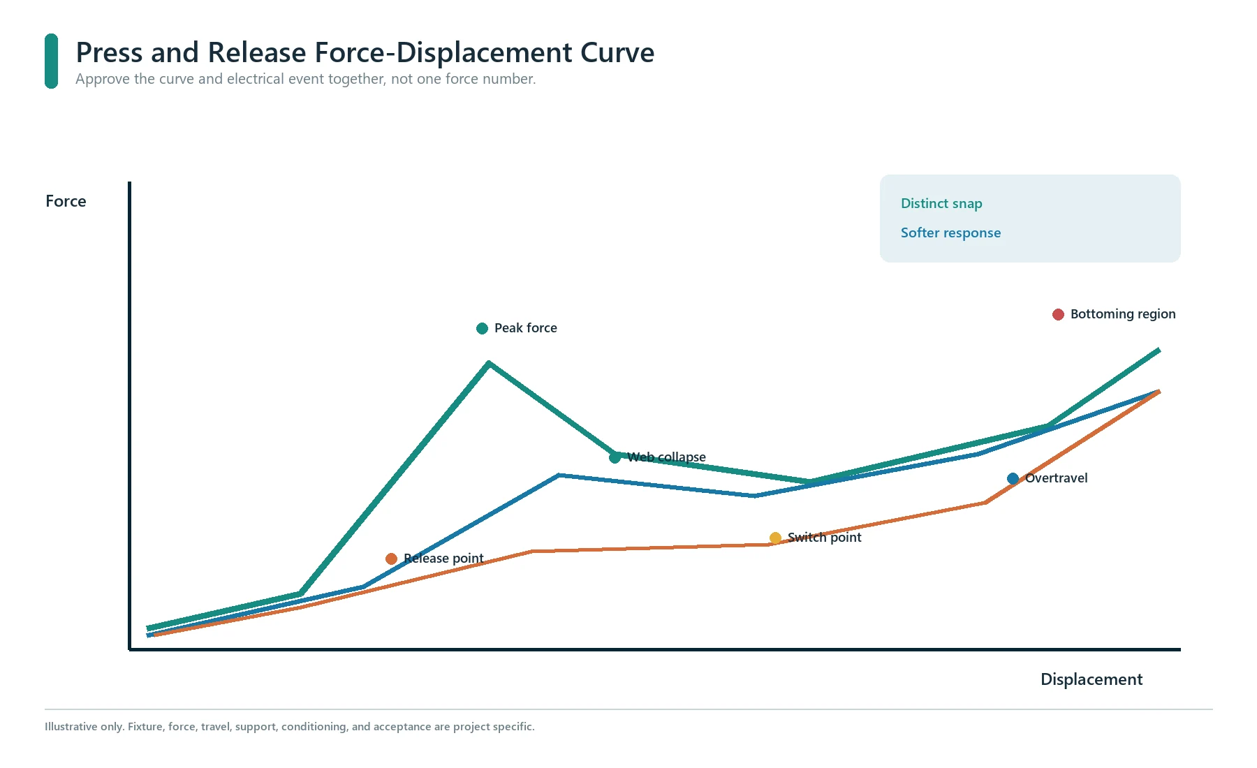
Actuation force is one point on a mechanical event. A useful approval curve records force against key displacement during both press and release.
Force
  ^
  |                    A peak force
  |                   /\
  |                  /  \____ C bottoming region
  |                 / B contact and overtravel
  |________________/________________________> Displacement
         start          switch point

Release follows a different return path and should also be recorded.
Industry keypad design references use force, travel, and tactile response together rather than treating one number as a complete specification.[5][6] The exact curve must come from the production-intent key, material, contact, PCB, support, and enclosure stack.
Peak force
Peak force is the highest load before the molded web rolls or collapses into the main travel region. It strongly affects the operator’s first impression, but it does not prove that the electrical contact has closed.
Contact force and switch point
The switch point is where the circuit meets the defined electrical condition. For a carbon-pill key, the mechanical and electrical traces should be captured together. The circuit may close before, near, or after the most obvious tactile event depending on geometry and stack.
Overtravel and bottoming
Overtravel is controlled movement available after electrical actuation. It can keep the contact closed while the user’s force varies and can reduce a sharp collision with the board. Too little may produce a fragile switching window. Too much may overload the pill, PCB, coating, web, or support.
The enclosure or support structure should provide an intentional hard stop when the design needs one. The PCB must not become an uncontrolled spring.
Return force and release point
Return force must lift the key and separate the contact after the finger is removed. A key may feel acceptable on the downstroke yet release slowly because of material behavior, side friction, coating contact, enclosure interference, preload, contamination, or an unfavorable web shape.
Record the release point as well as the press point. The difference between them is part of the tactile hysteresis and affects repeated operation.
Snap ratio is descriptive, not a universal pass limit
Keypad engineers often describe snap by comparing the force drop after the peak with the peak force. A larger normalized drop can feel more distinct; a smaller drop can feel softer. That relationship is useful, but one snap-ratio target does not fit every key size, glove condition, application, or architecture.
Approve the complete curve shape rather than relying on a calculated ratio. Two keys can share a ratio while having different peak force, travel, bottoming, return, and electrical timing.
Set Key Roles Before Sharing One Force Target
A keypad rarely contains identical use cases. Divide the layout into functional groups:
| Key role | Operator expectation | Design review |
|---|---|---|
| Frequent navigation | Repeatable rhythm and low fatigue | Force spread, spacing, travel, release, adjacent-key isolation |
| Confirm or emergency action | Deliberate actuation and clear identity | Force distinction, size, color, guard, switch timing |
| Numeric or data entry | Similar response across a group | Key-to-key curve consistency, pitch, wobble, legend alignment |
| Glove-operated control | Easy location without visual search | Key top area, separation, sculpting, force under the real glove |
| Hidden service function | Protection from accidental use | Recess, guard, alternate force, access method |
| Illuminated status key | Feel plus controlled optical output | LED position, light block, legend stack, thermal and color review |
Do not assign a single force because it is convenient for the drawing. If keys have different functions, document whether their response should match or intentionally differ.
Key Geometry Controls More Than Appearance
Key-top shape controls finger location
Flat, concave, convex, rimmed, angled, and sculpted key tops place the finger differently. The top must also carry a legend, texture, coating, and possibly a lighted area. Review it with the expected finger or glove, viewing angle, key spacing, and product orientation.
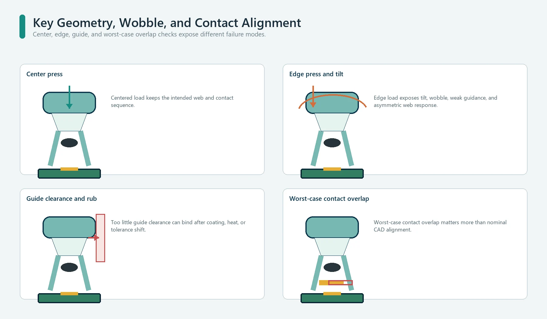
A tall key with a narrow guide can feel unstable. A wide top on a weak web can tilt under edge loading. A very small top can concentrate force and wear. Use center, edge, and corner presses during sample review.
Guide features control wobble and rubbing
Key walls, skirts, housing pockets, ribs, or molded guide posts may keep the key moving along the intended path. Their clearances must accommodate molding variation, coatings, temperature, contamination, and enclosure tolerance.
Too much clearance permits rocking. Too little creates rubbing or binding. The best clearance cannot be chosen from the keypad CAD alone because the mating housing establishes the other half of the guide.
The web is the molded spring
The thin rubber region around or below the key carries most of the elastic deformation. Its thickness, angle, length, curvature, symmetry, and transition radii influence peak force, snap, travel, return, fatigue, and tool release.
Small geometry changes can produce large force-curve changes. Therefore:
- dimension the web from controlled datums;
- avoid ambiguous surface-to-surface dimensions;
- identify which profile controls the force;
- keep fillets and transitions in the released model;
- do not let cosmetic CAD cleanup alter the spring; and
- approve measured curves from molded parts.
The key center must land where the circuit expects it
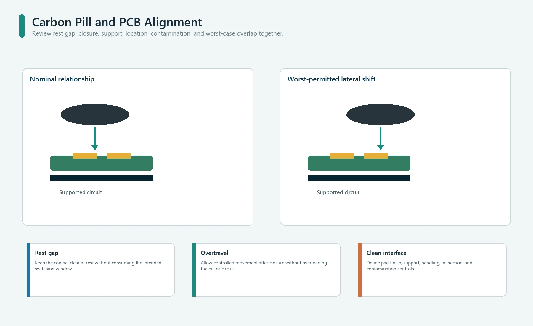
The molded contact or actuator needs positive alignment with the PCB pad, dome, or switch. Key tilt, rubber shrinkage, PCB movement, housing clearance, and assembly tolerance all consume overlap.
Review the worst-permitted lateral position instead of relying on the nominal overlay in CAD. Locating pins, holes, bosses, perimeter walls, or carrier frames should reference the keypad and circuit to a shared datum system.
Shore Hardness Does Not Specify Key Feel
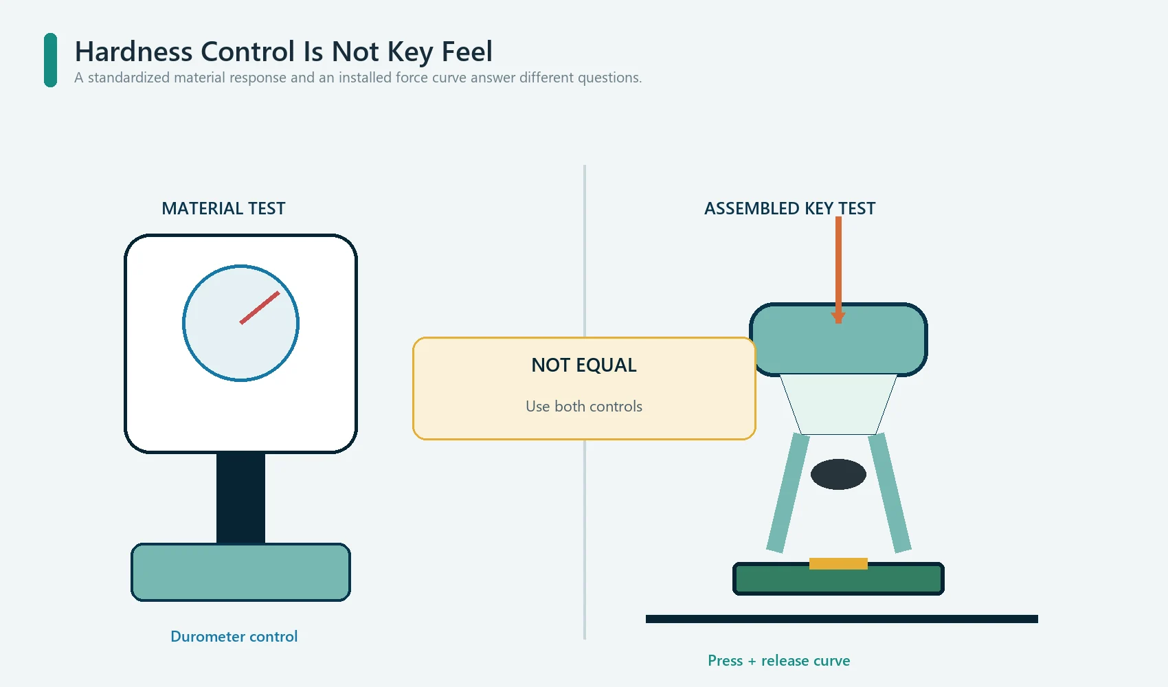
ASTM D2240 defines standardized durometer procedures for rubber hardness, with different durometer types used for different material ranges.[3] It is a material test. It does not measure the assembled force-displacement curve of a key.
A harder compound does not automatically create the preferred tactile response, and a softer compound does not automatically create lower actuation force. Web geometry, key area, travel, contact height, support, preload, and cure condition can dominate the result.
Use hardness in the specification for:
- incoming or batch material control;
- comparison with the approved material system;
- supplier change control; and
- investigation when molded behavior shifts.
Use a force-displacement test for key feel. Keep the test fixture, press point, speed, support, temperature, conditioning, and electrical state controlled.
WACKER’s material and processing guide shows that silicone families cover broad property and process ranges, while final shrinkage and other behavior depend on material grade and processing conditions.[1] Shin-Etsu likewise documents compression set, flex fatigue, tear behavior, transparency, coloring, weather, moisture, and chemical response as separate properties.[2] No single material label substitutes for the project validation plan.
Compression Set Matters Where Rubber Stays Loaded
ASTM D395 covers standardized methods for measuring how rubber retains deformation after a defined compressive exposure.[4] In a keypad project, the concept is relevant to perimeter seals, preload zones, supports, and any key that is held partly depressed by the enclosure.
It does not directly predict key life. A key web experiences repeated, geometry-specific flexing, while a compression-set specimen is tested under a defined compression condition.
Investigate unintended preload when:
- keys sit below their drawing position after assembly;
- release force drops in the installed product;
- one side of the keypad changes feel after fasteners are tightened;
- the seal lip is crushed beyond its intended range;
- a coating rubs the housing only after warm storage; or
- the PCB or support bows toward the keypad.
The drawing should distinguish the sealing compression path from the key actuation path.
Design the Conductive Contact as an Interface
For a carbon-pill architecture, define at least:
- pill outline and location;
- mating circuit pad outline;
- nominal and worst-case overlap;
- distance from pill to board at rest;
- electrical closure criterion;
- force and travel at closure;
- permitted overtravel;
- board finish and cleanliness requirement;
- test voltage/current where relevant; and
- resistance acceptance and sampling plan.
The detailed resistance target, pad pattern, contamination controls, and lifecycle method should be reviewed with the circuit owner. They will be developed in the dedicated carbon-pill article rather than generalized here.
Do not measure only a loose pill. The useful result is the contact behavior of the molded key on the specified circuit under the specified support.
Coordinate Legends, Coatings, Color, and Backlighting
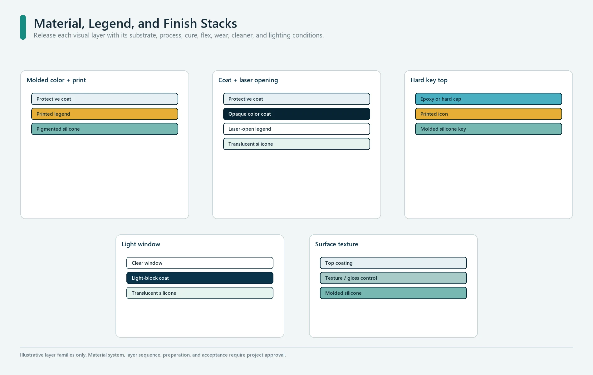
Silicone can be formulated in translucent or pigmented systems, and supplier literature describes its ability to accept color.[1][2] The final visual system, however, may include molded color, printed ink, sprayed color layers, laser removal, protective coating, light-blocking features, and an LED circuit.
Printed legends
Printing can suit non-illuminated marks and color details. Review ink adhesion, coverage, alignment, edge quality, surface texture, key flexing, finger wear, cleaners, oil, and UV exposure. A visually correct first sample is not a wear qualification.
Coated and laser-etched legends
A common illuminated construction uses a translucent base, one or more opaque color layers, and a laser-opened legend. The laser must remove the intended layer without producing an unacceptable edge, color shift, residue, or weak coating boundary.
The laser-etched silicone keypad route is appropriate when durable day/night legends are the commercial focus. For coating-stack selection and abrasion qualification, see laser-etched keypad legends and protective coatings.
Backlighting
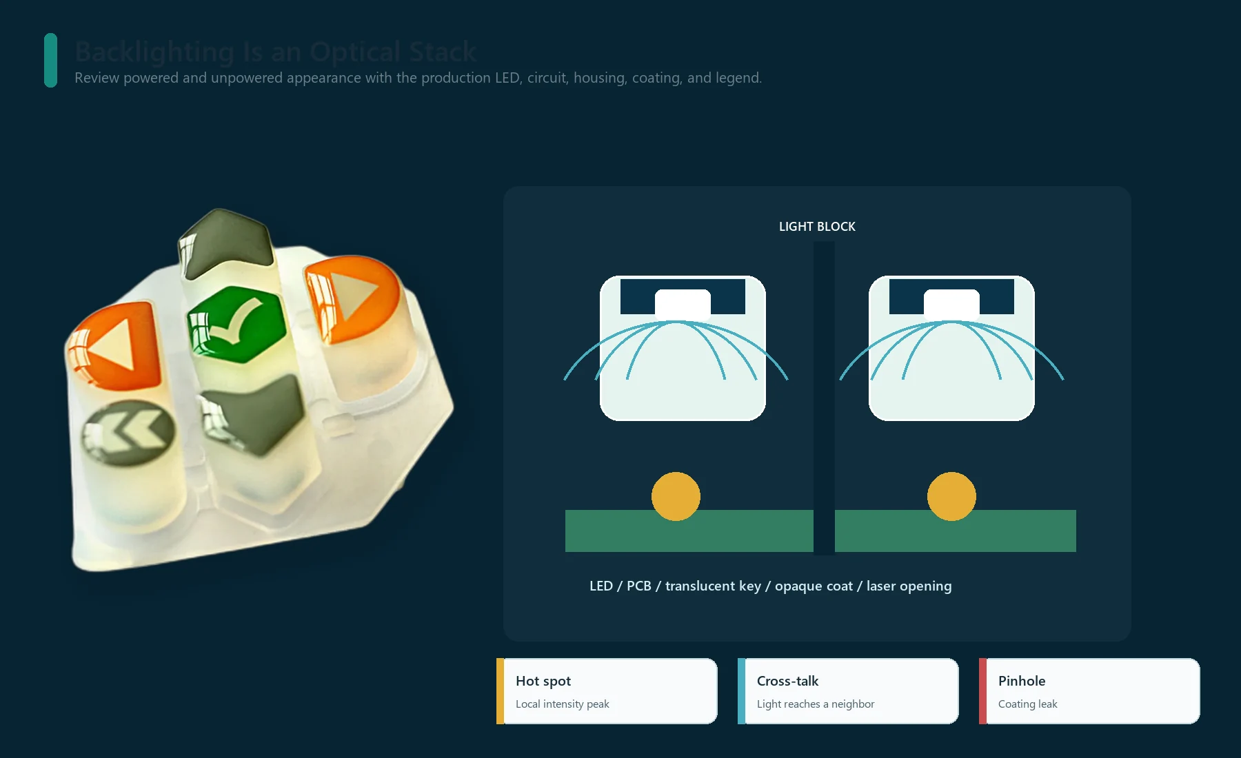
Backlighting is an optical stack, not an LED checkbox. LED position, distance, view angle, intensity, wavelength, keypad transmission, coating opacity, wall thickness, light-block ribs, PCB color, enclosure reflectivity, legend area, and neighboring keys all influence the result.
The backlit silicone rubber keypad route should be reviewed with the production-intent PCB and housing. Approve powered samples in the real ambient-light conditions and at the intended drive settings.
Use a Material and Finish Decision Matrix
| Design choice | Primary purpose | What must be defined | Main validation risk |
|---|---|---|---|
| Base silicone compound | Molded spring, key body, seal or light path | Approved grade, color, hardness method, cure/post-cure status, compliance | Substitution changes force, dimensions, appearance or environment response |
| Molded pigment | Body color or light control | Color target, masterbatch/system, section thickness, lighting condition | Color shift across thickness, lot, cure or illumination |
| Pad or screen print | Surface legend and color detail | Ink system, pretreatment, artwork, cure, adhesion, wear test | Edge wear, poor adhesion, cleaner attack, flex cracking |
| Opaque color coating | Full key/body color and light block | Layer sequence, thickness control, masking, cure | Pinholes, light leak, rubbing, adhesion loss |
| Laser-etched legend | Controlled opening through an opaque layer | Laser artwork, layer stack, removal depth, edge criterion | Uneven transmission, weak boundary, residue, alignment |
| Protective top coating | Wear, chemical or friction control | Coating grade, coverage, texture, gloss, cure, test media | Feel change, cracking, peeling, cleaner incompatibility |
| Epoxy or hard key-top feature | Local gloss, icon protection or styling | Outline, height, edge, adhesion, key flex allowance | Hard edge, delamination, altered force or finger feel |
| Translucent window or light pipe | Light output | Optical area, wall, finish, LED geometry, light block | Hot spots, cross-talk, low contrast, color variation |
The chosen finish must be tested on the actual molded substrate. Surface preparation, cure, geometry, and flexing can affect adhesion.
Integrate the Keypad with the PCB and Enclosure
Use shared datums
The keypad, circuit, and housing need common locating features. Do not position a carbon pill from one enclosure edge and the PCB pad from an unrelated board edge without a tolerance analysis.
Define:
- primary, secondary, and tertiary location;
- clearance versus interference features;
- anti-rotation features;
- assembly sequence;
- fastener torque or compression control where relevant; and
- accessible inspection points.
Support the circuit beneath the contact
A conductive contact requires a stable reaction surface. Unsupported PCB or FPC movement changes travel and contact load. Add a support plate, housing rib, standoff, adhesive support, or other controlled reaction feature as the design requires.
Check component keepouts beneath and around each key. LEDs, resistors, connectors, solder joints, test points, and tall components can interfere with the rubber or create uneven support.
Control preload
The installed stack must leave every key at its intended rest position. Review housing compression, bezel contact, adhesive thickness, PCB height, screw sequence, gasket thickness, and thermal movement. A nominal CAD gap does not prove that the worst-permitted assembly remains free.
When purchasing wants one controlled module rather than separate parts, the silicone keypad assembly route can combine the molded keymat with circuit, lighting, connector, spacer, housing interface, and final functional test.
Treat Sealing as an Enclosure System
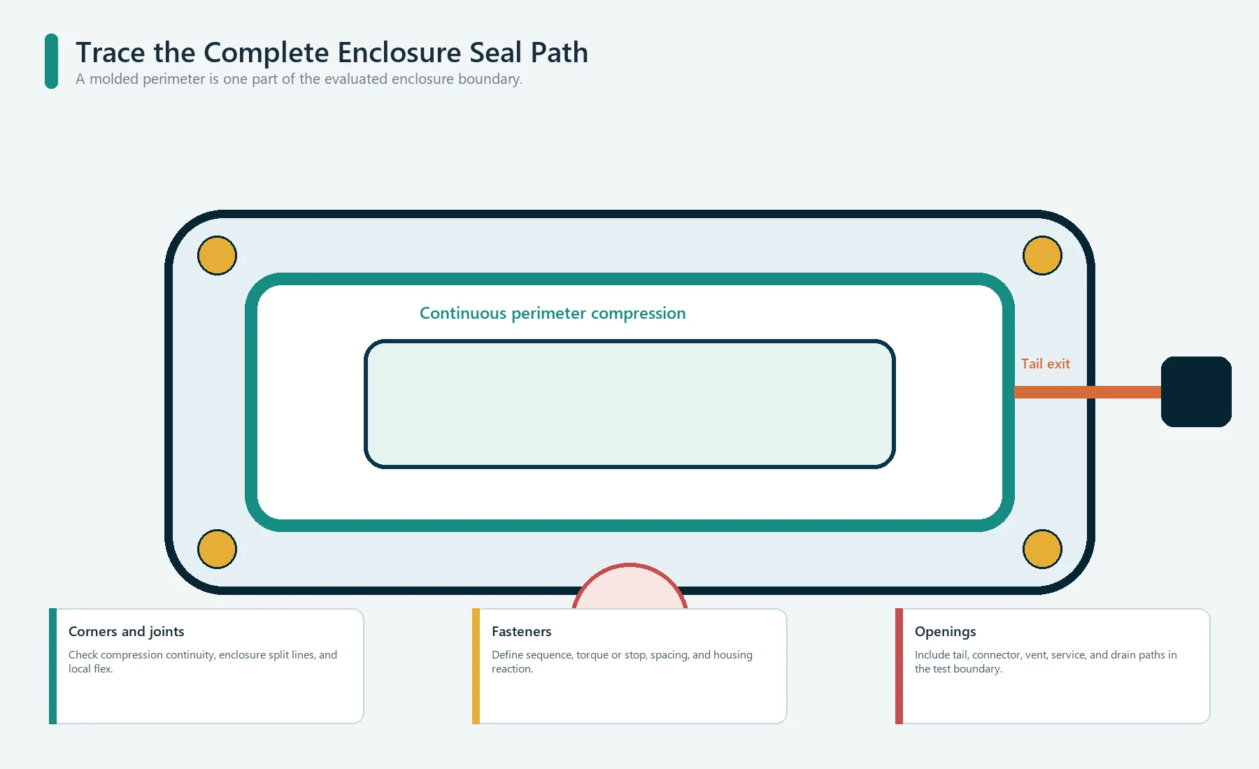
A molded perimeter lip can support sealing, but it does not assign an ingress rating to the loose keypad. IEC 60529 defines IP classification around the protection provided by an enclosure in its evaluated configuration.[7]
Draw the complete seal path:
external surface
  -> key field and molded perimeter
  -> compressed lip or gasket land
  -> corners, joints and fasteners
  -> PCB cavity
  -> cable, connector and vent exits
  -> enclosure halves and service openings
Specify:
- sealing land width and finish;
- compression target and hard stops;
- corner geometry;
- fastener location and sequence;
- tail or cable exit;
- drainage and pooling direction;
- enclosure deflection;
- assembly lubricant or contamination limits;
- service opening and resealing method; and
- test configuration and acceptance evidence.
Do not use the same thin web as an uncontrolled sealing spring if actuation and gasket compression pull it in conflicting directions.
Release Tooling Only After the Process Route Is Clear
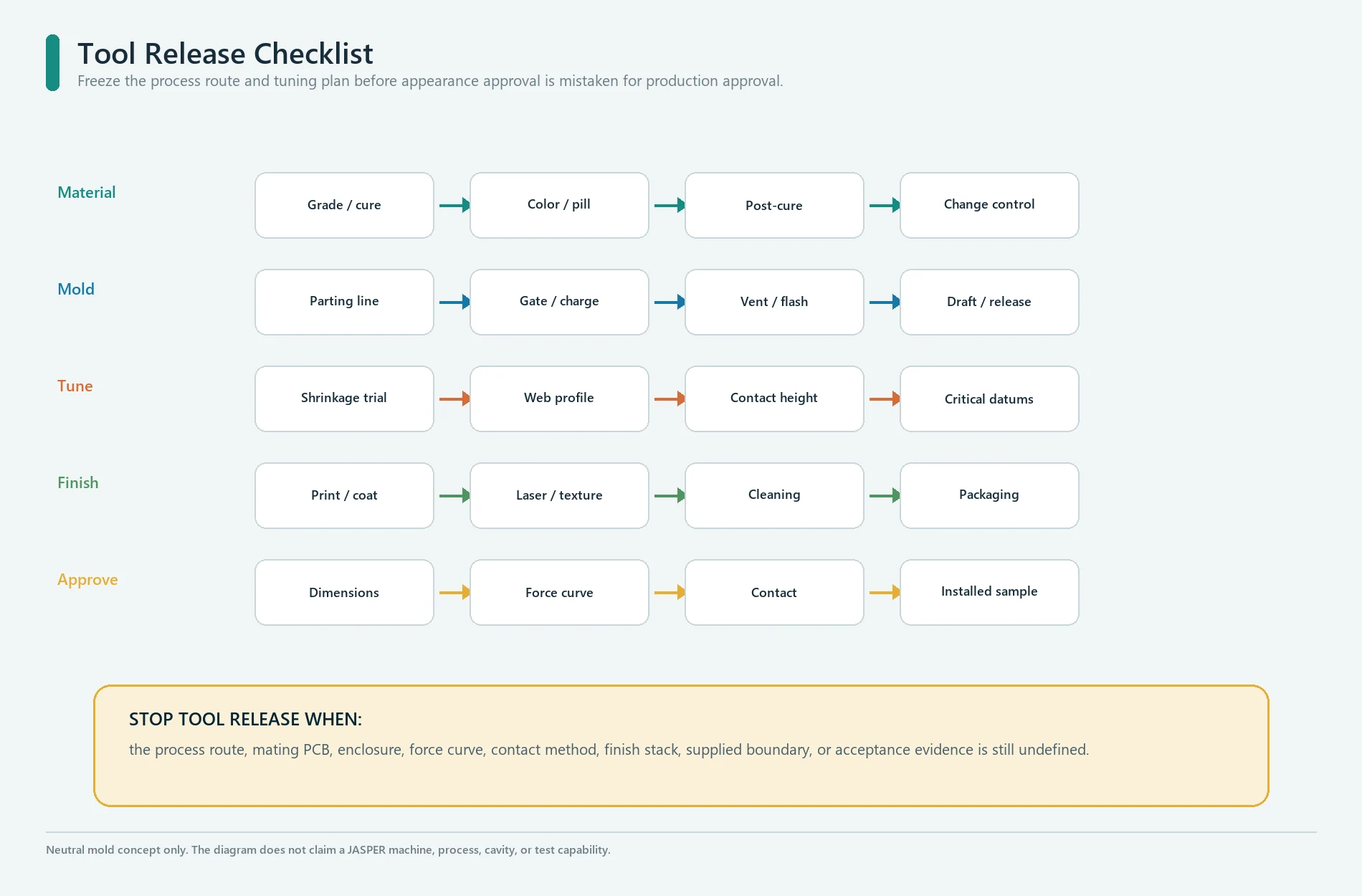
WACKER documents compression, transfer, and injection molding as distinct silicone processing routes, each with different material, tool, production, and economic considerations.[1] The keypad drawing should not assume that every silicone compound and geometry can move between those routes without change.
Before tool release, confirm:
- approved material family and cure route;
- mold concept and cavity count;
- parting-line location;
- gate or charge strategy;
- venting and trapped-air risks;
- flash limits and removal method;
- draft and demolding direction;
- undercuts and flexible pull-off features;
- texture and polish;
- insert or conductive-pill loading;
- shrinkage compensation method;
- post-cure requirement;
- color and coating sequence; and
- critical dimensions that will be tuned after first samples.
Material guides show that final shrinkage depends on material grade and processing conditions, so precision parts need preliminary trials and adjustment.[1] Do not write a universal shrinkage percentage into a new keypad drawing because another project used it.
Keep tooling approval separate from appearance approval
An attractive first shot may still have the wrong force curve. A mechanically acceptable keymat may still need color, print, coating, laser, or light correction. Keep mechanical, electrical, visual, and process approvals visible as separate gates.
Build a Controlled Keypad Drawing Package
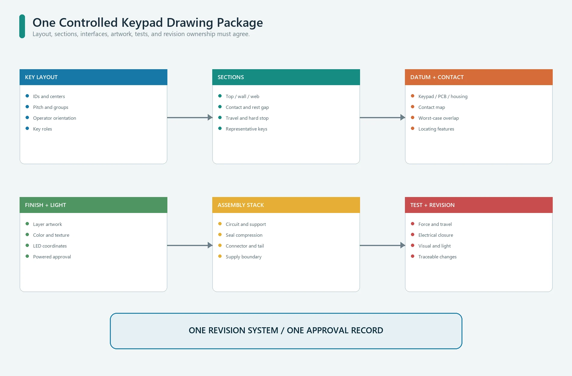
The released package should include more than one rendered view.
| Drawing element | Required content | Approval question |
|---|---|---|
| Key layout | Key IDs, centers, pitch, grouping, orientation | Can the operator locate and distinguish the controls? |
| Key sections | Top, wall, web, contact, rest gap, travel, hard stop | Does each representative geometry create the intended curve? |
| Datum scheme | Keypad-to-PCB-to-housing references | Can production reproduce contact and legend alignment? |
| Contact map | Pill/actuator locations, pad references, circuit ownership | Does every key land within worst-case overlap? |
| Material specification | Grade, color, hardness method, cure status, compliance | Is substitution controlled? |
| Finish artwork | Legend layers, colors, coating, laser, texture, tolerances | Can visual inspection use an objective reference? |
| Lighting package | LED coordinates, drive condition, light blocks, legend zones | Is the powered appearance approved in context? |
| Assembly stack | PCB/FPC/PET, spacer, adhesive, connector, housing and support | Is rest height and preload controlled? |
| Test requirements | Force curve, travel, contact, resistance, light, visual, seal | Is sample and lot acceptance repeatable? |
| Revision record | Customer, supplier and mating-part revisions | Can a later change be traced to the approved system? |
Use a 3D model for complex molded surfaces, but keep inspection dimensions and acceptance notes in a controlled 2D drawing. A model without datums and test requirements is not a complete production specification.
Dimension Functional Relationships
Not every surface needs a tight tolerance. Tighten the dimensions that control:
- key center to contact center;
- contact to PCB pad overlap;
- rest gap and switch point;
- web profile;
- key top to housing clearance;
- hard-stop position;
- perimeter seal compression;
- LED to optical feature;
- legend to key top;
- keypad locator to PCB locator; and
- connector or tail exit.
Use tolerance analysis for relationships that cross parts. Avoid solving an assembly problem by applying unnecessarily tight tolerances to the entire rubber part.
When a molded dimension is intentionally tuned after first samples, mark the release state clearly. The approved production model must capture the final geometry rather than leaving it only in supplier notes.
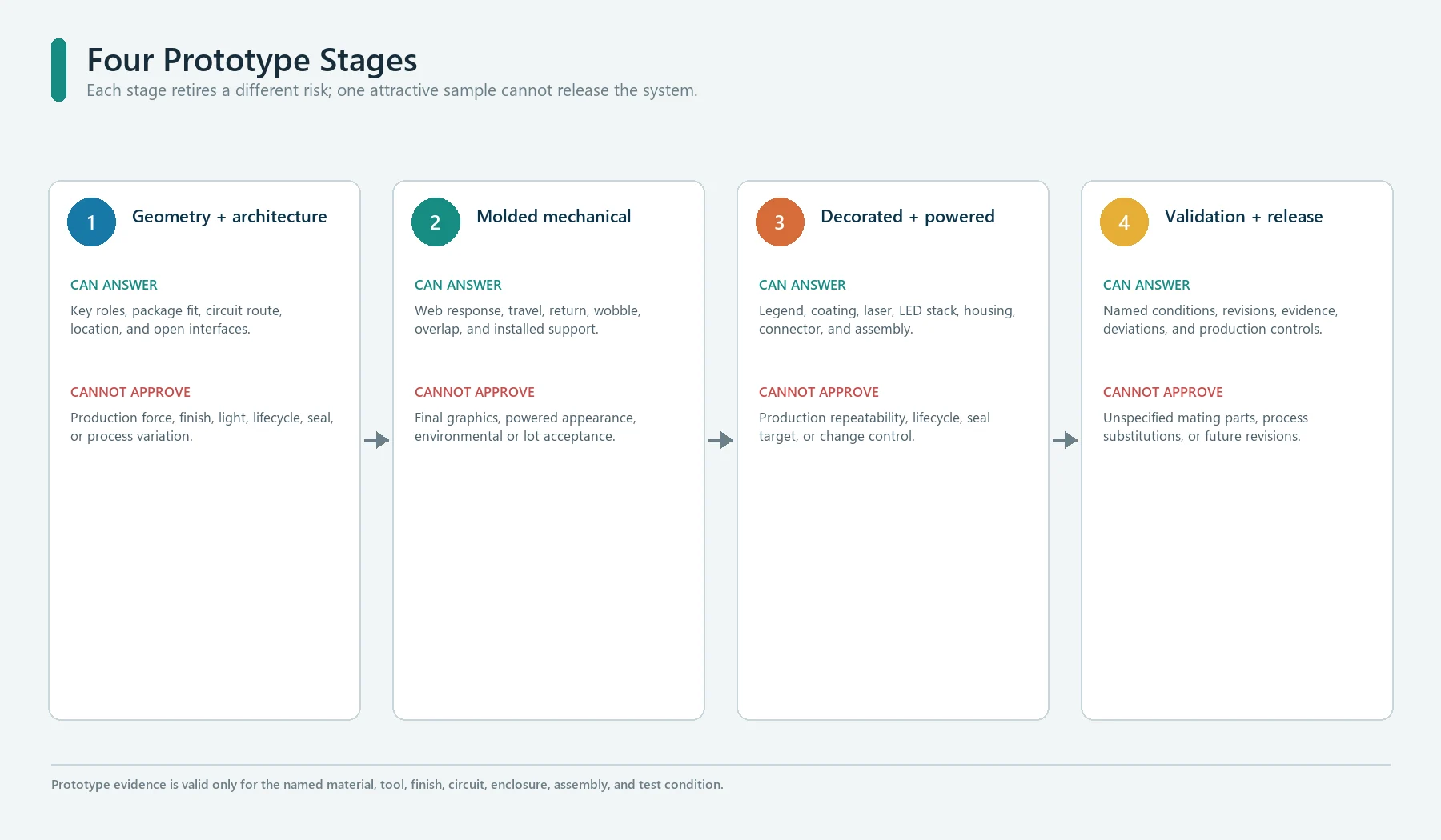
Prototype the Installed System
JASPER’s current prototyping page describes prototype work as a way to confirm fit, function, appearance, feel, lighting, and assembly before repeat production. For a silicone keypad, use staged evidence:
Stage 1: geometry and architecture check
Review key size, spacing, enclosure fit, PCB location, contact method, optical zones, and the intended force path. A non-production model may answer fit questions but cannot approve molded force or final coating.
Stage 2: molded mechanical sample
Measure key position, representative dimensions, force-displacement curves, wobble, return, and contact timing. Record material, tool revision, cure, conditioning, fixture, support, and test settings.
Stage 3: decorated and powered assembly
Add production-intent print, coating, laser, LEDs, PCB/FPC/PET, connector, housing, fasteners, and seal compression. Review feel, electrical behavior, appearance, light output, cross-talk, and assembly sequence together.
Stage 4: validation and production release
Run the agreed environmental, cleaner, abrasion, cycling, ingress, transport, and functional tests on traceable revisions. Convert accepted results into drawings, work instructions, inspection criteria, and change-control records.
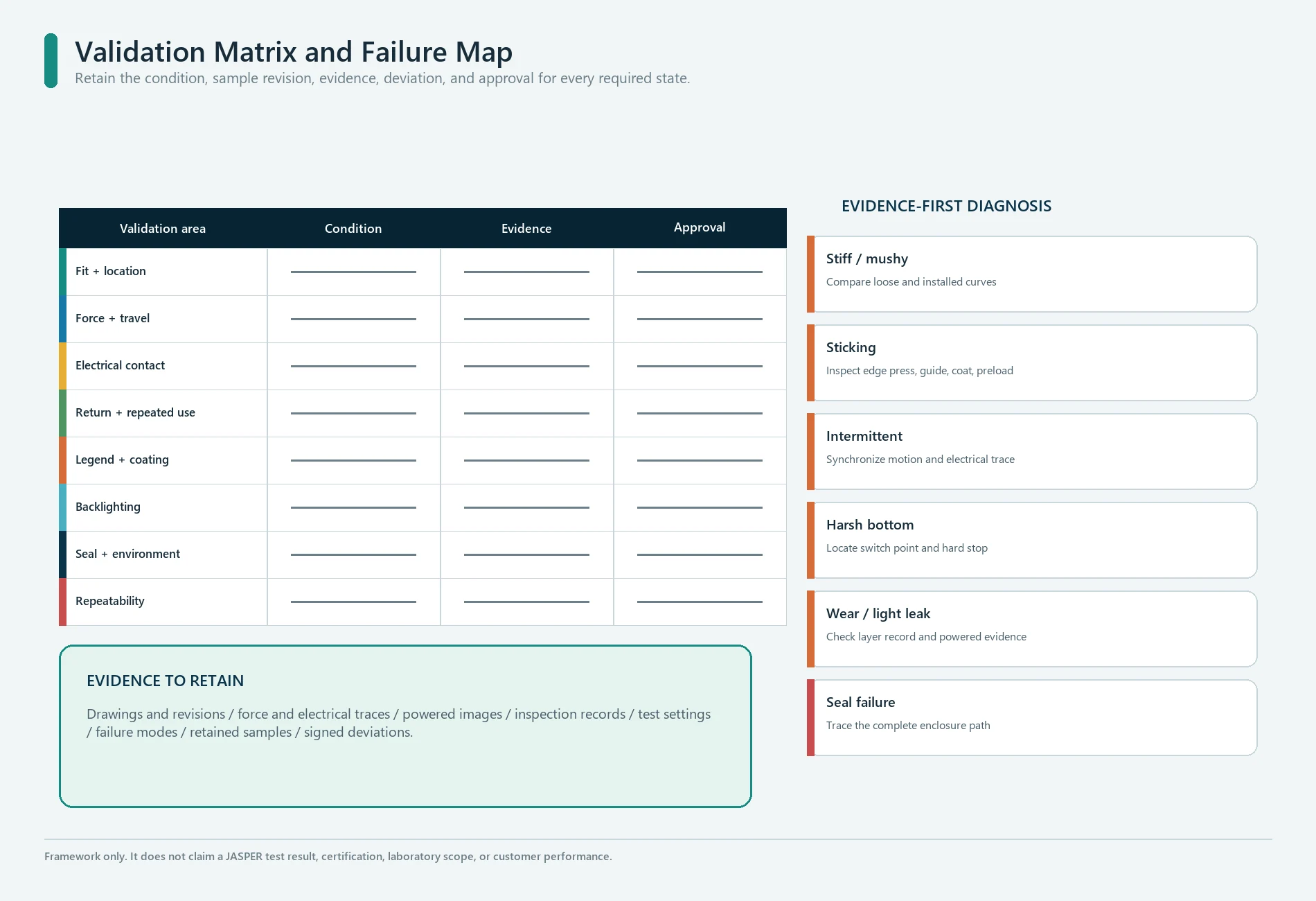
Use a Validation Matrix Instead of a Sample Photo
| Validation area | Production-intent condition | Evidence to retain |
|---|---|---|
| Fit and location | Specified housing, PCB, support, fasteners and assembly sequence | Dimensional report, installed photos, interference review |
| Force and travel | Controlled fixture plus assembled product | Press/release curves by key group, test settings, sample revision |
| Electrical switching | Specified circuit, pad, support and test signal | Closure point, resistance/result, bounce or timing if required |
| Return and repeat use | Center and edge press, repeated sequence, warm/cold state where required | Release curves, sticking or slow-return observations |
| Legend and coating | Production ink/coating/laser stack | Artwork revision, visual limits, adhesion, wear and cleaner results |
| Backlighting | Production LEDs, drive setting, housing and ambient condition | Powered images, luminance/color method if specified, light-leak limits |
| Seal and environment | Complete enclosure and production assembly | Test configuration, exposure, pre/post checks, deviations |
| Lifecycle | Defined key groups, load path, rate, environment and pass criteria | Cycle count, periodic measurements, failure mode, retained samples |
| Manufacturing repeatability | Multiple cavities/lots where applicable | Cavity identity, force/dimension spread, inspection records |
The matrix should state sample quantity, conditioning, revision, pass criterion,
measurement method, and owner. Avoid a vague requirement such as test for durability.
The industrial control keypad case study is useful for its enclosure, glove, legend, connector, adhesive, and inspection questions. It does not prove that a membrane-keypad result transfers unchanged to molded silicone; the keypad architecture still needs its own validation.
Inspect the Characteristics That Can Drift
Production inspection should connect back to function:
| Characteristic | Why it can matter | Practical control direction |
|---|---|---|
| Key and base dimensions | Fit, guide clearance, rest height, seal compression | Drawing-based dimensional inspection |
| Web and critical profile | Force, travel, return, fatigue | Tool/process control plus representative section or curve |
| Hardness | Material/cure consistency | Standardized durometer method on an appropriate specimen |
| Force-displacement curve | Operator feel and switch sequence | Controlled fixture, key groups, cavity/lot sampling |
| Contact position | Pad overlap and closure | Visual/dimensional check against shared datum |
| Electrical result | Switching stability | Defined circuit and test method |
| Print/coating/laser | Readability, wear, light control | Approved visual standard and process-specific tests |
| Backlight output | Hot spots, cross-talk, contrast | Powered fixture and defined ambient condition |
| Cleanliness | Contact, coating and cosmetic risk | Handling, inspection and packaging controls |
| Assembly stack | Preload, support, connector and LED function | Functional fixture and assembly record |
Do not let one golden sample become the only specification. Samples age, color perception changes, and hidden geometry cannot be judged from appearance.
Diagnose Failures from Evidence
| Symptom | Possible system causes | Evidence to collect first |
|---|---|---|
| Key is too stiff | Web geometry, compound, contact height, enclosure preload, support | Loose and installed curves, dimensions, material/tool revision |
| Key feels weak or mushy | Low peak/drop, excess flex, missing support, long travel | Full press/release curve, board movement video, section measurement |
| Key sticks down | Side rubbing, coating contact, preload, contamination, damaged web | Edge-press test, clearance, warm-state inspection, surface evidence |
| Uneven key feel | Different geometry, cavity/process spread, housing distortion | Key/cavity map, curves, fastener sequence, flatness |
| Intermittent switching | Pill-pad misalignment, insufficient closure, contamination, board flex | Mechanical/electrical synchronized trace, overlap, cleanliness |
| Harsh bottoming | Contact closes late, no overtravel, hard stop misplaced | Switch point versus force curve, stack height, contact gap |
| Legend wears | Incompatible ink/coating, poor preparation, wrong test media | Layer record, adhesion/wear result, cleaner list |
| Light leaks between keys | Coating pinhole, wall transmission, LED position, reflective housing | Powered dark-room and ambient images, layer/LED inspection |
| Seal fails | Incomplete path, wrong compression, enclosure flex, tail exit | Compression map, fastener state, leak path, complete assembly |
Change one controlled variable at a time. A geometry correction can affect force, contact, light, seal, and tool release at once.
Know When Silicone Is Not the Best Interface
Choose another architecture when:
- the complete interface must remain extremely thin and flat;
- the front graphic changes frequently between product variants;
- a continuous wipe-clean film is more important than raised key shape;
- discrete sealed mechanical switches already satisfy the force and lifecycle requirement;
- a dynamic display and coordinate touch surface are required; or
- project volume, tooling plan, or revision risk does not support molded parts.
For a thin printed laminate with metal-dome or non-tactile switching, review the membrane switch design guide and the membrane keypad manufacturer route. Do not force a silicone keymat into a product whose main requirement is a flat, thin graphic surface.
Stop Tool Release When an Interface Is Undefined
Pause the project when:
- the PCB contact layout is not controlled;
- the target force is stated without travel or a curve;
- the enclosure support and hard stop are missing;
- the customer cannot identify the supplied assembly boundary;
- the material grade may change after sampling;
- the legend or coating stack is still undecided;
- backlighting is requested without an LED board and drive condition;
- an IP target is assigned to the loose keypad;
- the seal compression depends only on screw feel;
- production tests have no acceptance criteria; or
- the mating PCB, enclosure, or connector revision is likely to change after tooling.
A tooling schedule does not reduce the risk created by missing inputs. It only makes later corrections more expensive.
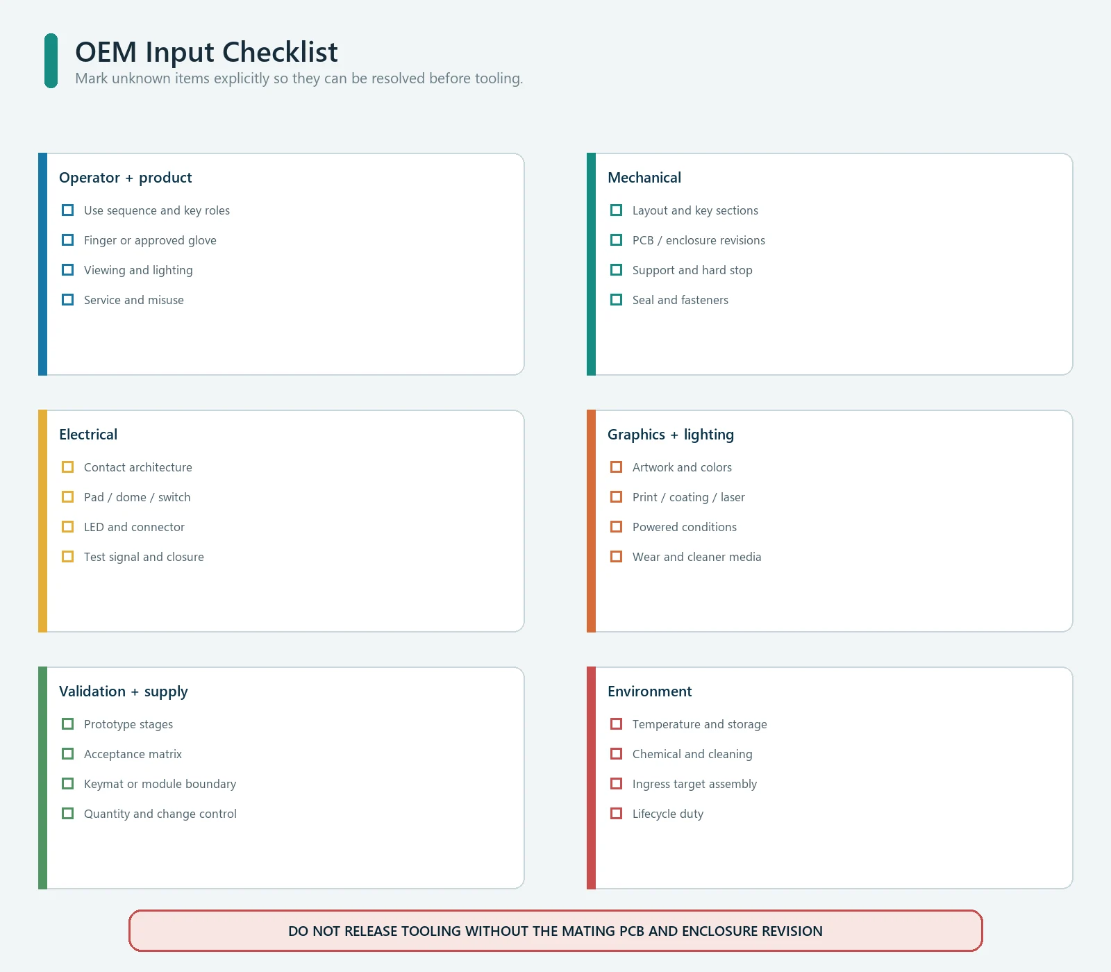
OEM Input Checklist
Send the following for an engineering and quotation review:
Product and operator
- application and product location;
- user, glove and operating posture;
- frequent, safety-related and infrequent key groups;
- indoor/outdoor, cleaning, oil, dust, water, UV and temperature exposure; and
- required compliance or customer specifications.
Mechanical
- 2D drawing and 3D model;
- enclosure pocket, support and fastening details;
- key centers, pitch, top shape, height and guide features;
- target force-displacement curve, travel and return behavior;
- permitted wobble and edge-press behavior;
- hard stop and overtravel plan;
- seal path and compression control; and
- prototype and annual quantities.
Electrical
- contact architecture;
- PCB/FPC/PET or switch drawing;
- contact-pad location and finish;
- carbon-pill or actuator requirement;
- resistance, timing or signal requirements;
- LED, component and keepout layout;
- connector, pinout and cable/tail route; and
- electrical test method.
Graphics and lighting
- color references and viewing condition;
- molded color, print, coating and laser artwork;
- surface texture and gloss;
- legend wear and cleaner exposure;
- LED type, position, drive condition and ambient-light use;
- light-leak and cross-talk limits; and
- cosmetic acceptance samples or defect criteria.
Approval and supply
- supplied boundary: keymat only or assembled module;
- customer-owned mating parts and revisions;
- required sample stages;
- validation matrix and lifecycle duty;
- inspection reports and traceability;
- packaging and cleanliness requirements; and
- change-notification and requalification rules.
Frequently Asked Questions
What determines the feel of a silicone rubber keypad?
The complete molded and installed system determines feel: compound, key area, web geometry, travel, contact height, overtravel, hard stop, PCB support, enclosure preload, guide clearance, coating, conditioning, and test method. Shore hardness alone is not a key-force specification.
What should a keypad force specification contain?
Specify the press and release force-displacement curves, switch point, travel, peak force, overtravel, bottoming behavior, return point, test fixture, press location, speed, conditioning, support, and permitted variation by key group.
Can a carbon pill keypad be approved without the final PCB?
It can be evaluated mechanically, but the electrical interface cannot be fully approved without the intended pad geometry, finish, support, alignment, signal condition, and installed stack. A representative circuit coupon may be useful before the final board is available.
Does a higher Shore A hardness make the key more tactile?
Not by itself. Hardness measures a material response under a standardized durometer method. Key tactility comes from the force drop, travel, geometry, contact sequence, support, and return behavior of the assembled key.
How should backlit keypad samples be approved?
Use the production-intent silicone, color/coating/laser stack, LEDs, board, drive settings, housing, light blocks, ambient conditions, and viewing angles. Approve hot spots, cross-talk, legend transmission, unlit appearance, color, and key feel together.
Can the molded keypad provide an IP rating?
The keypad may contribute a perimeter seal, but an IP rating applies to the evaluated enclosure configuration. The test assembly must include the housing, compression land, fasteners, tail/connector exits, joints, vents, and service openings.
Should every key use the same geometry?
Only when the operator function and desired response are the same. Navigation, confirm, emergency, glove, numeric, service, and illuminated keys may justify different size, shape, force, travel, guard, or color.
What is the minimum package needed for a useful quote?
Provide the layout, key count, enclosure/PCB relationship, target feel, contact method, graphics, lighting, environment, supplied boundary, validation requirements, prototype quantity, annual volume, and launch timing. Mark unknown items so they can be resolved before tooling.
Sources
- WACKER, Solid and Liquid Silicone Rubber – Material and Processing
Guidelines:
https://www.wacker.com/h/medias/6709-EN.pdf - Shin-Etsu Chemical, Characteristic Properties of Silicone Rubber
Compounds:
https://www.shinetsusilicone-global.com/catalog/pdf/rubber_e.pdf - ASTM International, ASTM D2240, Standard Test Method for Rubber Property –
Durometer Hardness:
https://store.astm.org/d2240-15r21.html - ASTM International, ASTM D395, Standard Test Methods for Rubber Property –
Compression Set:
https://store.astm.org/d0395-18r25.html - Epec, Silicone Rubber Keypads:
https://www.epectec.com/keypads/ - Epec, Rubber Keypad Design Guide:
https://www.epectec.com/keypads/design/ - IEC, IEC 60529, Degrees of Protection Provided by Enclosures (IP Code):
https://webstore.iec.ch/en/publication/2452
Source notes support the relationships and test concepts above. Material, force, travel, resistance, environment, life, coating, light, seal, tolerance, process, and compliance values remain project-specific unless they are stated in an approved JASPER drawing and validation plan.
Request a Silicone Keypad Design Review
Send the keypad layout or 3D model, PCB/contact drawing, enclosure section, target press and release behavior, graphics, lighting, environment, validation requirements, and expected volume through the JASPER RFQ form. Ask for the response in four parts: open design inputs, proposed supplied boundary, prototype evidence, and production acceptance plan.