
OEM capacitive interface engineering resource
Custom Capacitive Touch Panel Design Guide
A custom capacitive touch panel should be designed from the installed product inward, not from finished artwork backward. Define the operator, functions, touch architecture, cover stack, active and view areas, display, electrode carrier, controller, tail, connector, ground and shield, bonding, enclosure, feedback, environment, test states, and acceptance evidence before locking graphics or tooling.
JASPER’s custom capacitive touch panels can combine a printed or rigid cover, discrete touch zones or a larger sensing area, a PCB/FPC or other sensor construction, display and LED features, a connector, adhesive, gasket, and front-panel assembly. The quotation must still state who owns the controller, firmware, display, tuning, EMC work, equipment validation, and final regulatory approval.
What Is a Custom Capacitive Touch Panel?
A custom capacitive touch panel is the physical operator-interface stack built around a product-specific cover, sensing geometry, electrical connection, graphics, enclosure, and acceptance plan. It is not only the visible lens, only the electrode artwork, or only a generic touchscreen module.
The term can describe several different products:
| Buyer term | Practical meaning | Main design owner |
|---|---|---|
| Capacitive touch switch | One no-travel sensing zone below an icon | Button geometry, cover, controller, feedback |
| Capacitive touch keypad | Several discrete buttons, sometimes with sliders or a wheel | Zone spacing, routing, lighting, host behavior |
| Projected capacitive panel | A coordinate or multi-touch sensing area, often over a display | Active area, transparent sensor, controller, display integration |
| Capacitive HMI front | Cover, graphics, touch, display window, lighting, adhesive, gasket, and connection as one front assembly | Mechanical, electrical, optical, software, and validation teams |
| Cover lens only | Printed glass, acrylic, polycarbonate, or film without the sensing electronics | Appearance, fit, printing, bonding, and compatibility with the buyer’s sensor |
Write the purchased scope in the drawing and quotation. A cover-only project should not be described as a tuned touch assembly. A sensor-tail assembly should not be described as a complete HMI unless the display, controller, host, and installed behavior are included.
Start With the Installed System Boundary
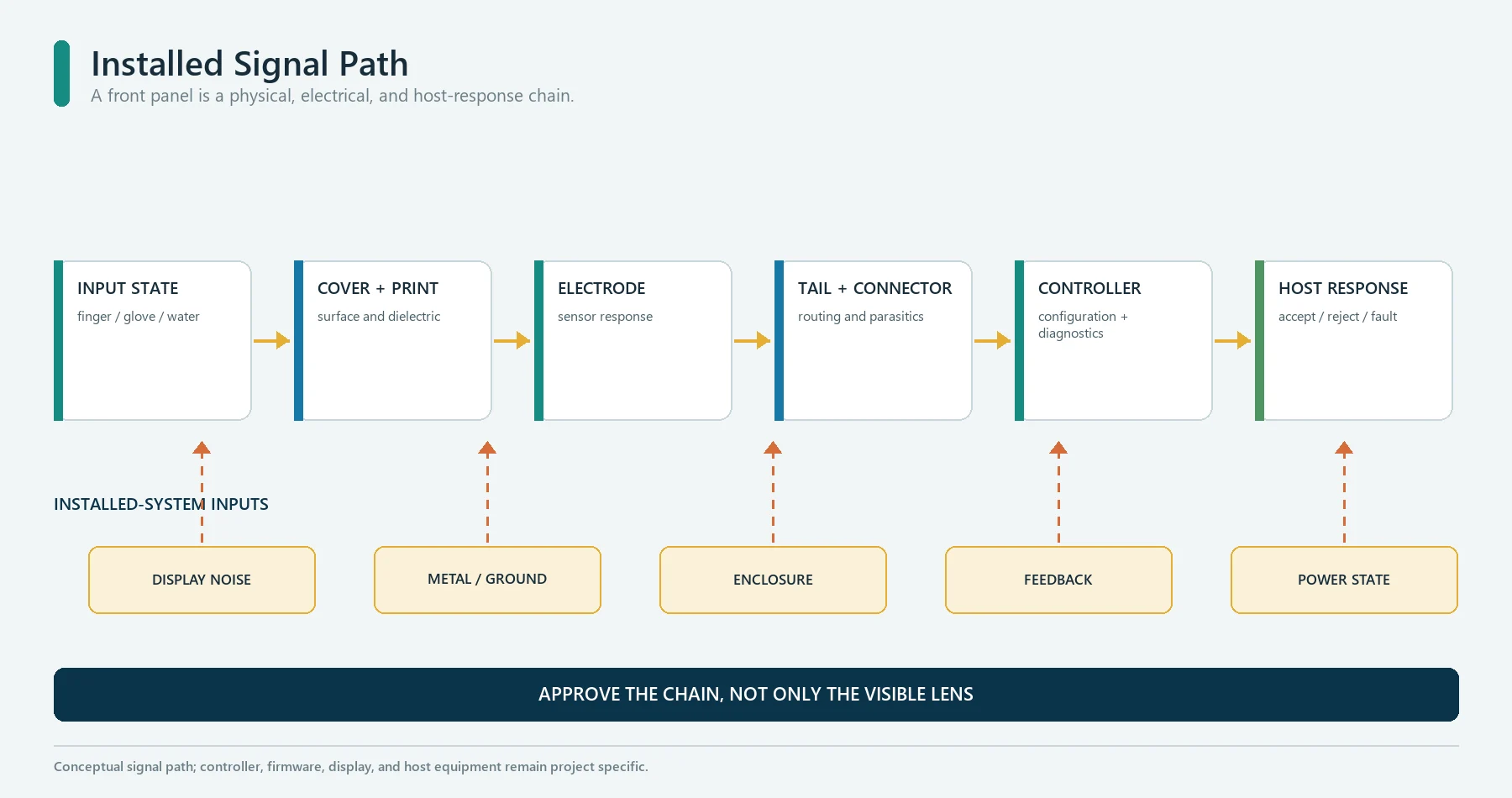
The front panel is one part of a signal path:
Operator, glove, stylus, water, or cleaning contact
                         |
                         v
Cover surface, coating, graphics, and dielectric stack
                         |
                         v
Touch electrode or coordinate sensor
                         |
                         v
Tail, connector, routing, ground, shield, and power environment
                         |
                         v
Touch controller, firmware, diagnostics, and host interface
                         |
                         v
Accepted command, rejected event, feedback, or fault response
The mechanical stack changes the electrical signal. The electrical design changes which mechanical stack is practical. The host behavior decides whether a detected event is useful, unsafe, or confusing. Review those boundaries in one design meeting instead of passing an artwork file between departments.
Assign responsibilities before layout
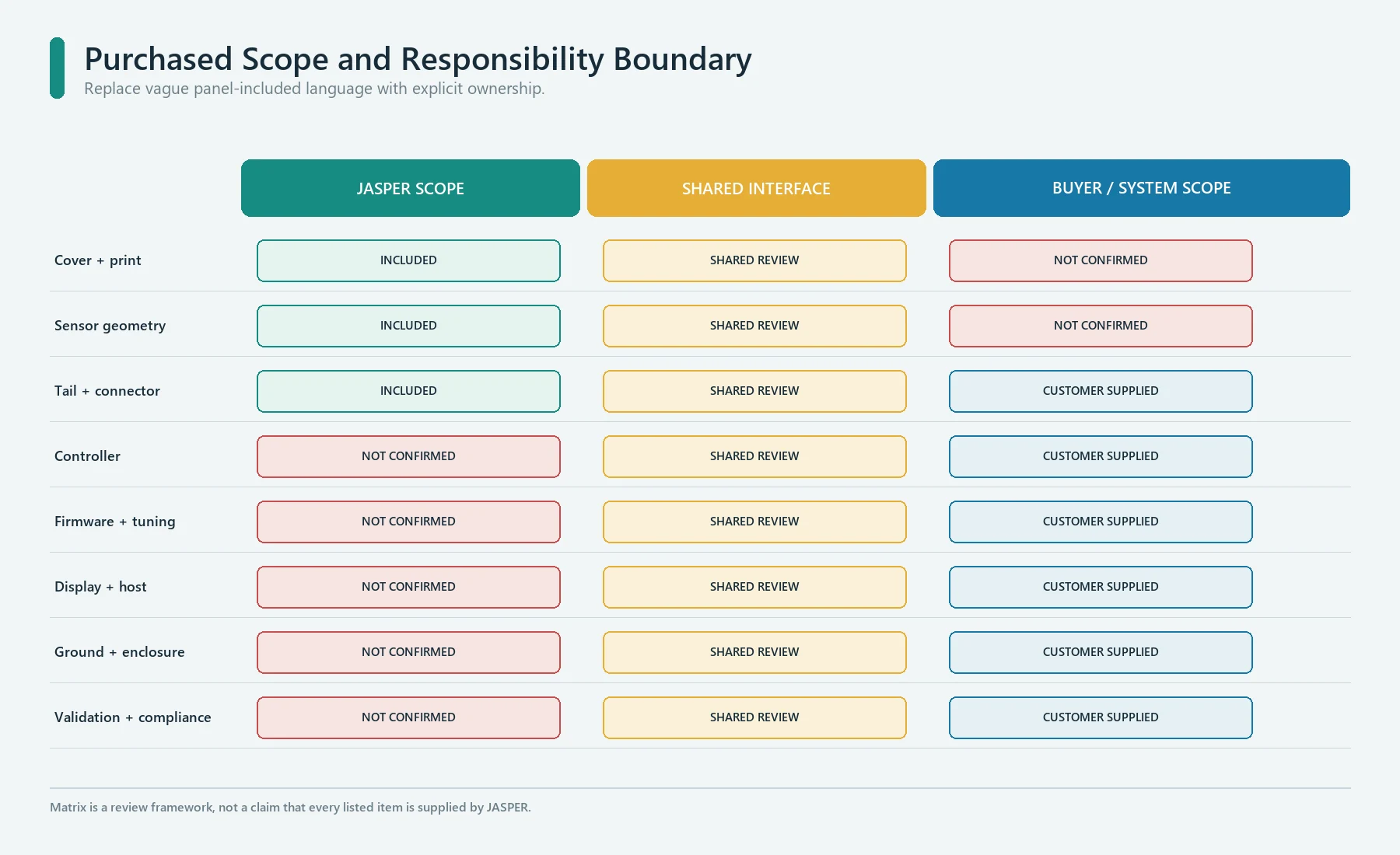
Use a responsibility table early:
| Work item | JASPER, buyer, or shared decision? | Evidence required |
|---|---|---|
| Cover material, printing, finish, cutouts | State in quotation | Approved material and artwork |
| Sensor construction and electrode layout | State in quotation | Controlled sensor drawing |
| Controller selection and tuning | State in quotation | Device, configuration, firmware revision |
| Display and optical stack | State in quotation | Display drawing and installed stack |
| Tail, connector, pinout, and cable route | Shared | Interface drawing and mating-part data |
| Ground, shield, chassis, and noise strategy | Shared | System schematic and enclosure data |
| Water, glove, cleaning, and false-touch behavior | Shared | State table and validation matrix |
| Final equipment compliance | Normally buyer/system owner | Applicable standard and passed system report |
Do not use touch panel included as a substitute for this table.
Choose the Sensing Architecture Before Artwork
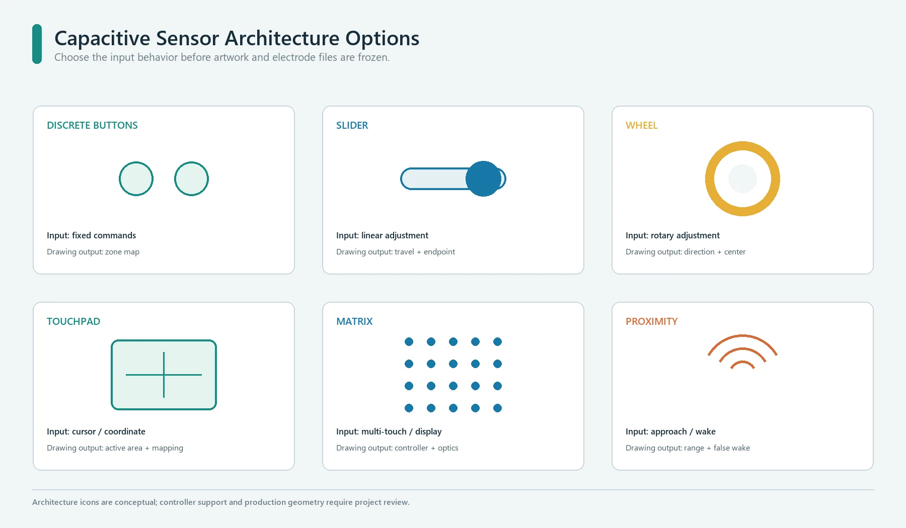
The visible icon does not determine the electrode architecture. Start with the required input.
| Required input | Common starting architecture | Questions to settle |
|---|---|---|
| One or more fixed commands | Discrete self- or mutual-capacitance sensors | Number of zones, spacing, simultaneous touches, feedback |
| Linear adjustment | Slider electrodes | Resolution, travel length, endpoint behavior, wet/glove use |
| Rotary adjustment | Wheel electrodes | Diameter, center exclusion, direction, acceleration, feedback |
| Cursor or coordinate entry | Touchpad or projected-capacitive matrix | Active area, coordinate resolution, controller, host mapping |
| Multi-touch or gesture input | Mutual-capacitance matrix and compatible controller | Touch count, gesture ownership, display mapping, noise budget |
| Proximity or approach detection | Dedicated proximity electrode and state logic | Range target, enclosure, ground, false wake-up behavior |
Microchip and Texas Instruments both treat sensor geometry, cover, routing, shielding, and controller behavior as linked design inputs rather than independent parts.[6][7] A controller reference layout can be a starting point, but it is not a production drawing for every cover, display, enclosure, or input condition.
Define Active Area, View Area, and Touch Targets Separately
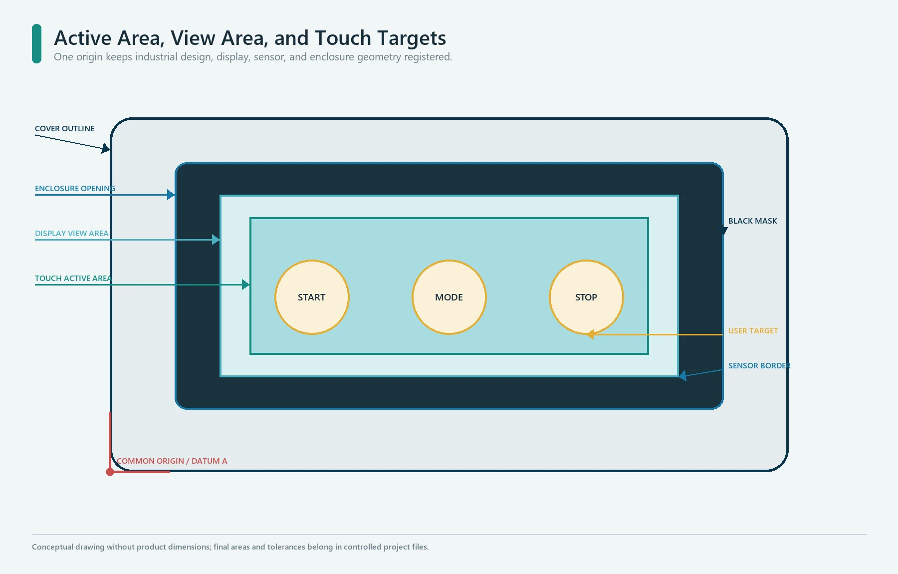
The words active area often hide three different geometries:
- Display view area: the visible image that must not be blocked.
- Touch active area: the region where coordinate sensing is valid.
- User touch target: the icon, button, slider, wheel, or gesture region presented to the operator.
There may also be a display active area, a clear aperture, a black-mask opening, a sensor border, a bezel overlap, an adhesive border, and a mechanical opening. These are not interchangeable.
Use one coordinate system
Choose a primary datum and origin. Dimension the following from that same reference:
- cover outline and corner radii;
- display view and active areas;
- touch active area;
- icon centers and touch targets;
- electrode or matrix origin;
- clear and printed windows;
- LED and dead-front features;
- adhesive and gasket borders;
- housing opening and bezel overlap;
- tail exit and connector orientation.
If the industrial-design artwork uses the cover center, the display drawing uses one corner, and the sensor file uses another origin, registration errors become likely even when each individual file is internally correct.
Include edge behavior in the requirement
A coordinate sensor may not have identical behavior at the center, edge, and corner. A discrete key close to a bezel, ground feature, metal wall, display edge, or another electrode can also behave differently. Define whether edge and corner targets are required, excluded, enlarged, or handled by the user interface. Do not approve only the easiest center touch.
Design the Cover Lens as Part of the Sensor
The cover is a dielectric layer between the user and the electrode. Its material, thickness, coating, print, adhesive, air gaps, curvature, and production variation all affect coupling.
Microchip documents that increasing cover distance reduces touch coupling and changes the electrode geometry needed for sensitivity.[6] The useful rule is the relationship, not a universal dimension. Electrode size must be designed for the selected controller, input object, cover stack, spacing, and noise environment.
Compare cover routes by the real product requirement
| Cover route | Useful when | Review before selection |
|---|---|---|
| Printed glass | A rigid optical window, hard front, second-surface graphics, or premium appearance is required | Edge treatment, impact target, weight, print, strengthening, bonding, display optics |
| Acrylic or PMMA | A rigid transparent plastic lens with machining and printing flexibility is preferred | Scratch protection, chemical exposure, optical needs, flatness, temperature, bond compatibility |
| Polycarbonate | Impact resistance and shaped plastic construction are important | Hardcoat, chemical list, optical quality, print, molding or machining, dimensional stability |
| PET or PC film overlay | A thin flexible printed face is supported by a rigid sensor or enclosure | Support flatness, adhesive, print stack, window clarity, handling, edge seal |
JASPER’s current capacitive touch switch guide introduces the broad cover, sensor, grounding, lighting, moisture, and enclosure questions. The present Resource goes deeper into the controlled drawing package and production transfer.
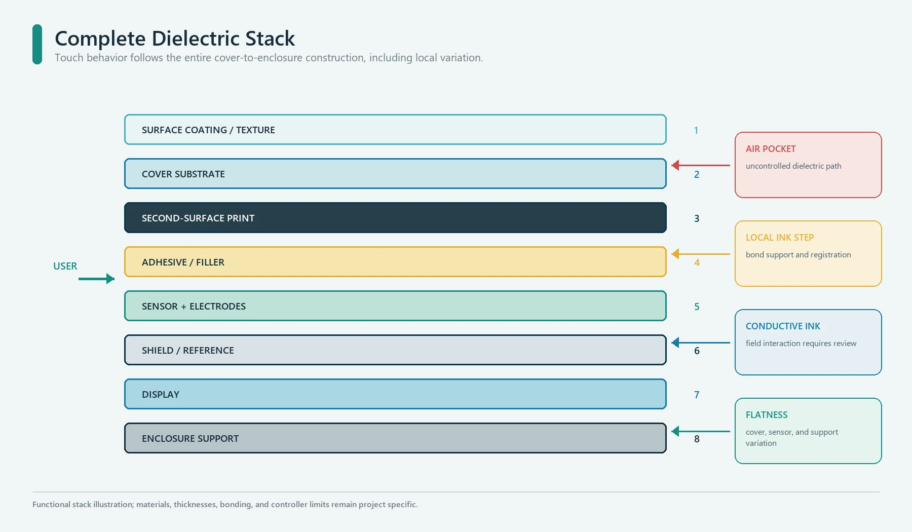
Specify the complete dielectric stack
Record more than the nominal cover:
User contact
    |
surface coating or texture
    |
cover substrate
    |
second-surface print, black mask, or dead-front ink
    |
adhesive, optical adhesive, filler, or intentional gap
    |
sensor substrate and electrodes
An alternate ink, label, adhesive carrier, protective film left in place, or local air pocket can change the stack. Texas Instruments notes that adhesives, labels, inks, transition materials, and air gaps belong in the capacitive mechanical design, and that the stack should remain non-conductive where the architecture expects a dielectric.[7]
Control Ink Borders, Windows, and Dead-Front Graphics
The artwork is functional geometry. It controls what the operator sees and can also change the local stack above the sensor.
Define:
- visible color and surface finish;
- second-surface or first-surface printing;
- black-mask and display-window boundaries;
- dead-front icon transmission in lit and unlit states;
- clear, tinted, diffused, or selective-texture regions;
- print registration to the cover, sensor, display, and LEDs;
- conductive, metallic, mirror, or specialty ink restrictions;
- allowable pinholes, edge light, halo, and cosmetic defects;
- color master, instrument method, and viewing condition where needed.
Metallic-looking graphics deserve an explicit material review. A visual effect that uses conductive material can interact with the electric field differently from an ordinary non-conductive print. Do not let a late decorative substitution enter production without electrical review.
Keep the icon and the electrode as separate controlled layers
The icon center should align with the intended touch target, but the electrode does not need to copy every decorative outline. The electrode is designed for coupling and separation. The artwork is designed for communication. Lock their relationship through common datums rather than by turning one file into the other.
Eliminate Uncontrolled Air Gaps and Bond Variation
An air gap is not simply empty space in a mechanical drawing. It changes the dielectric path and may vary across the panel. Texas Instruments identifies eliminating unintended low-dielectric air gaps as a main stack-up objective.[7]
Review:
- whether bonding is full-surface, perimeter, local, or absent;
- whether the sensor is supported against the cover;
- adhesive thickness and tolerance;
- local print steps and ink build;
- cutout and window transitions;
- dust, wrinkles, bubbles, trapped moisture, and liner removal;
- cover and sensor flatness;
- assembly pressure and cure conditions;
- rework method and damage risk.
An intentional display air gap can be valid. An uncontrolled sensor-to-cover gap is a different problem. Give each gap a function, nominal stack, tolerance, and inspection method.
Design Electrodes Around the Real Stack
Do not approve an electrode pattern before the cover, input object, controller, ground environment, and adjacent features are known.
Discrete buttons
Check:
- touch target and likely fingertip contact;
- cover stack and local print;
- sensor size and shape;
- distance to neighboring sensors;
- edge and bezel proximity;
- trace connection;
- LED holes or backlighting;
- ground, shield, display, and metal below or around the sensor;
- glove, wet, cleaning, and accidental-contact states.
Making a sensor larger is not a universal cure. It can change parasitic capacitance, adjacent coupling, spatial selectivity, and water response. Use controller guidance and measured design margin.
Sliders and wheels
Specify the usable travel, resolution, direction, end behavior, center or dead region, interpolation method, and feedback. Review the complete electrode pitch and crossover behavior with the cover stack. A decorative ring or line is not a slider specification.
Coordinate and transparent sensors
For a display touch area, define:
- touch and display active-area relationship;
- border and routing zone;
- sensor orientation;
- connector side;
- transparent conductor or sensor construction;
- optical stack;
- controller channel and matrix compatibility;
- coordinate origin, rotation, and host mapping;
- edge and corner accuracy requirements;
- allowed occlusion, pattern visibility, haze, and cosmetic criteria.
The electronics and industrial-design teams must agree on portrait/landscape rotation and coordinate direction before firmware integration.
Keep Traces, Tail, and Connector From Becoming Unplanned Sensors
Sensor connection lines carry small capacitive signals. Their length, geometry, neighbors, substrate, connector, and noise exposure contribute to the electrical design.
Texas Instruments recommends short sensor connections where practical and notes that connectors add parasitic capacitance and a noise-placement tradeoff.[7] That does not mean every remote sensor is impossible. It means the tail and connector must be designed as part of the sensing circuit.
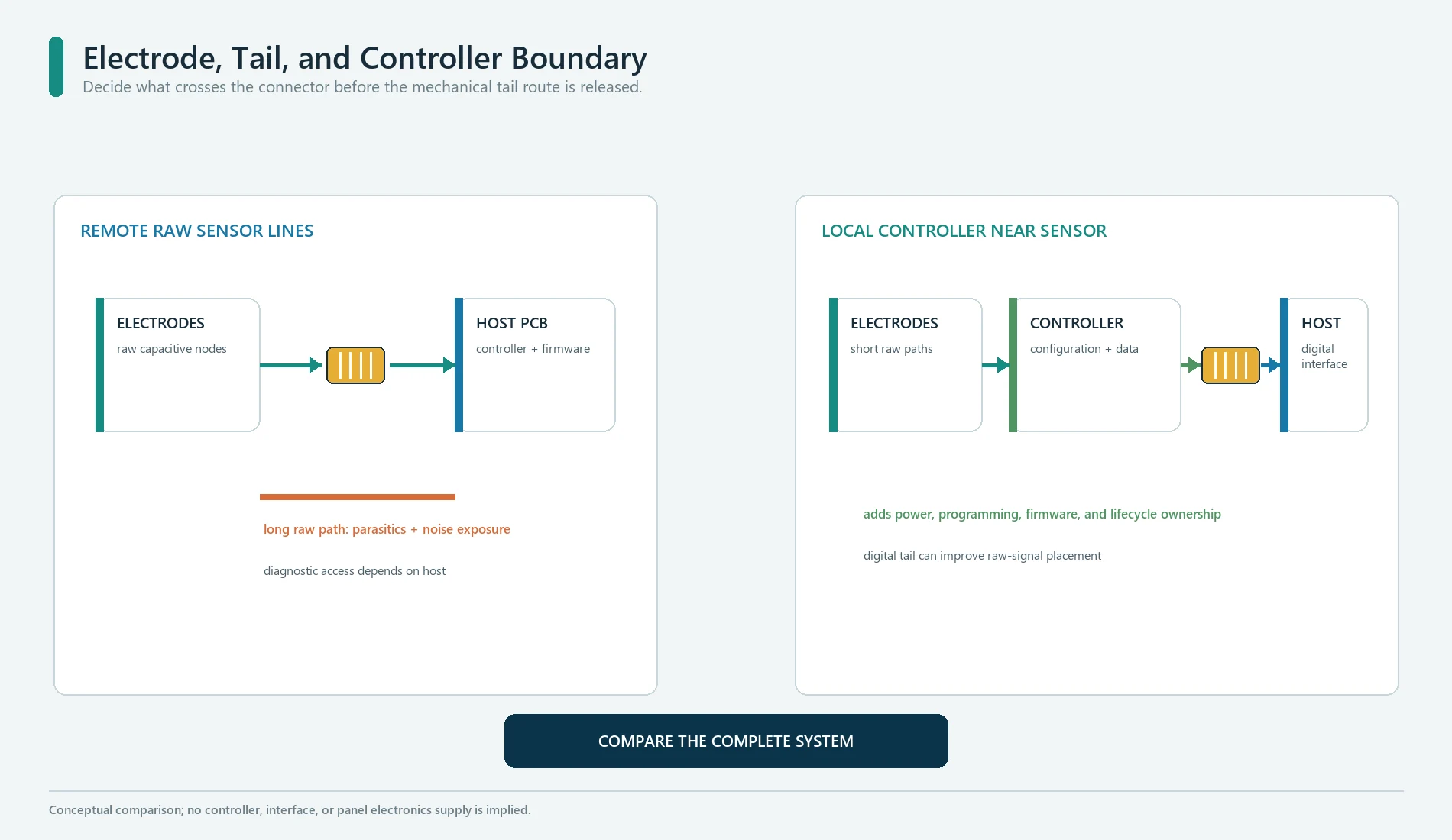
Decide what crosses the tail
Two common boundaries are:
Remote raw sensor:
electrodes -> tail/connector -> controller on host PCB

Local touch controller:
electrodes -> nearby controller -> power and digital interface to host
The first may simplify the panel electronics but exposes raw sensor lines to tail length, connector, host layout, and system noise. The second can shorten sensor paths but adds controller placement, power, firmware, programming, diagnostics, and assembly responsibility to the panel. Compare both before the mechanical tail route is frozen.
Put these details on the tail drawing
- substrate and copper or conductor construction;
- number and function of conductors;
- contact side and connector orientation;
- pin numbering and mating connector;
- stiffener, exposed contact, and insertion region;
- minimum allowed bend region from the selected construction;
- dynamic versus one-time bend use;
- keepouts, folding direction, and adhesive restrictions;
- strain relief and enclosure pinch points;
- shield or ground features where applicable;
- tail exit seal and service route;
- electrical test points and continuity criteria.
Do not copy a membrane-switch tail detail onto a capacitive sensor without checking its effect on the sensing and controller architecture.
Choose Controller Location and Interface Ownership Early
The controller is not a purchasing afterthought. It determines sensor support, channel count, self- or mutual-capacitance options, scanning behavior, noise features, tuning tools, communication, diagnostics, update method, and production programming.
Record:
| Controller decision | What to document |
|---|---|
| Device and variant | Exact part or approved alternative list |
| Sensor mapping | Electrode-to-channel assignment and reserved channels |
| Power | Supply, startup, sleep, wake, and brownout behavior |
| Host interface | I2C, SPI, UART, GPIO, interrupt, or other agreed interface |
| Firmware ownership | Source, binary, programming, versioning, and change approval |
| Configuration | Baseline, thresholds, filters, state logic, and production file |
| Diagnostics | Raw data, status, fault, reset reason, and test access |
| Calibration | Factory, startup, field, or fixed configuration boundary |
| Update path | Connector, bootloader, fixture, or no-field-update decision |
If JASPER supplies only the physical panel, the buyer must supply controller constraints before sensor release. If a controller board or programmed assembly is included, the quotation must define firmware, programming, test, and lifecycle responsibility.
Review Display, Ground, Shield, Metal, and Noise Together
A design that passes on an isolated bench can fail near the production display, charger, motor drive, radio, metal bezel, chassis, or cable.
Microchip describes shielding as a way to reduce unintended activation from EMI or touches on non-target traces and regions.[6] Shield type and drive method are controller-specific. A ground plane, passive shield, active shield, guard, and chassis connection are different tools.
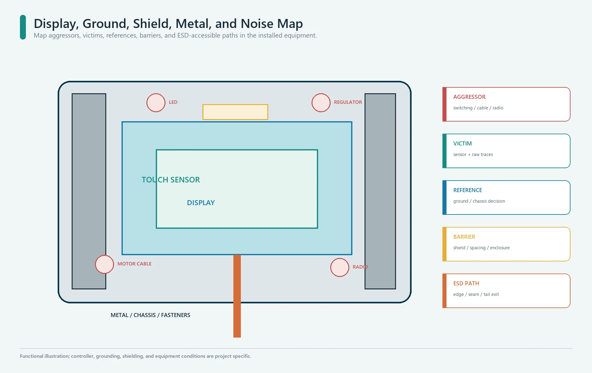
Create a noise and conductor map
Mark on one assembly drawing:
- display outline and electronics;
- high-current LED and backlight routes;
- switching regulators;
- motors, relays, heaters, radios, antennas, and high-speed lines;
- metal bezel, chassis, fasteners, brackets, and decorative metal;
- ground and shield connections;
- ESD-accessible edges, seams, ports, and tail exits;
- sensor traces and controller;
- cables that move between test and installation.
Then identify which items are aggressors, victims, references, or barriers. Do not add a ground pour everywhere by habit; nearby ground can also reduce sensitivity and change the electric field.
Treat EMC and ESD as installed-equipment tests
The panel can support an immunity strategy through cover, routing, shielding, grounding, controller choice, filtering, and enclosure design. Final EMC and ESD performance belongs to the complete powered equipment and its applicable product standard. A passed continuity or touch-function check is not an EMC qualification.
Integrate Lighting and Operator Feedback With Touch
A capacitive key has no inherent travel or snap. The design needs visible, audible, haptic, or host feedback appropriate to the task.
ISO 9241-210 treats hardware and software as parts of the same human-system interaction lifecycle.[8] For a touch panel, that means sensor detection and host feedback should be validated as one operator experience.
Coordinate:
- LED location and current route;
- light guide, diffuser, reflector, and light-blocking layers;
- dead-front icon transmission;
- display animation or state change;
- audio or haptic confirmation;
- feedback latency;
- accepted, rejected, disabled, wet, cleaning, and fault states;
- night mode and unintended light leakage;
- sensor routing around lighting features.
The capacitive touch control-panel case framework shows why overlay, sensor, lighting, enclosure, grounding, and buyer electronics must be reviewed together. It is a planning framework, not proof of a universal touch or lighting result.
Define Water, Gloves, Cleaning, and Environment as Test States
Works wet and works with gloves are not drawing requirements. Name the
actual states:
- approved bare and gloved input objects;
- dry, damp, wet, contaminated, and aged glove conditions;
- droplets, film, runoff, pooling, condensation, wipe, and drying recovery;
- cleaning material, method, duration, and lockout behavior;
- operator posture and target location;
- temperature, humidity, power, display, and enclosure conditions;
- required accepted, rejected, disabled, and fault response.
This Resource records those states in the design package but does not prescribe a universal threshold or glove mode. The controller, sensor, cover, ground, enclosure, state logic, and installed validation must support the agreed behavior.
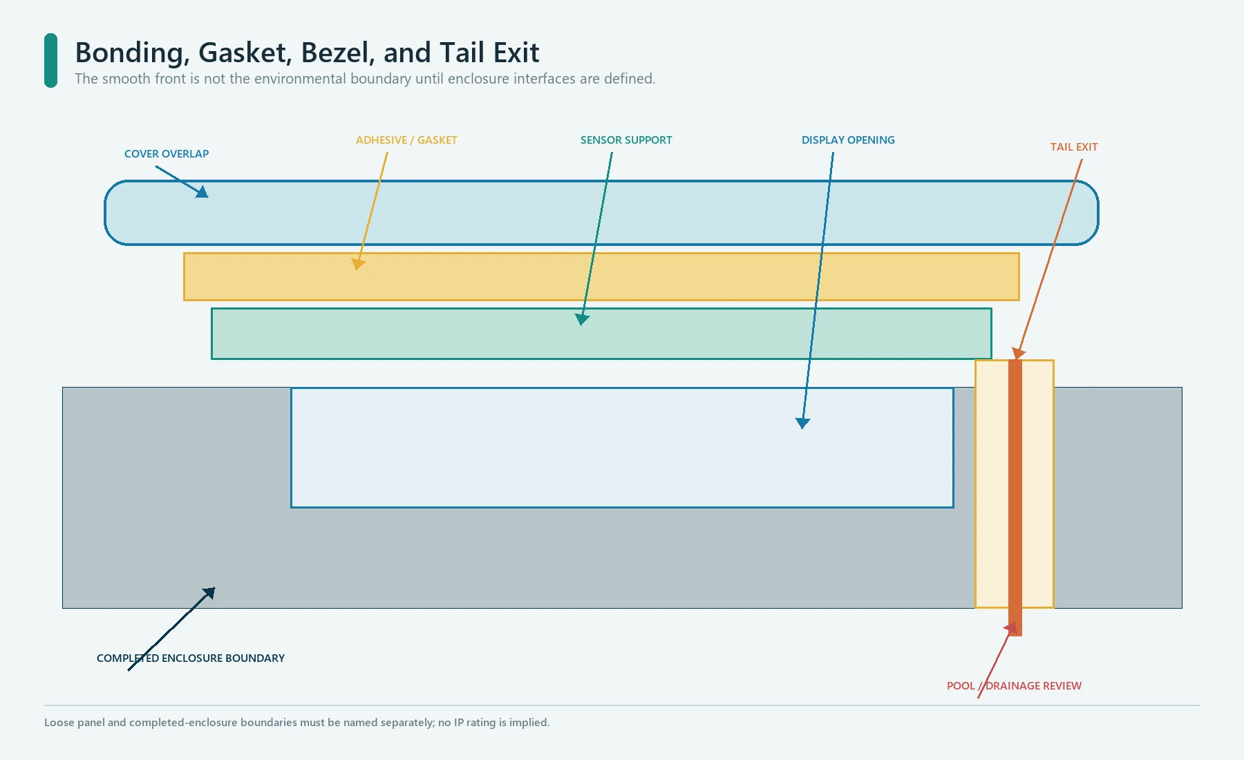
Design Bonding, Gasket, Bezel, and Tail Exit as One Boundary
The smooth front surface is not automatically an environmental seal.
Define:
- cover overlap and bezel support;
- adhesive or gasket geometry;
- compression and assembly sequence;
- housing material and surface preparation;
- corners, cutouts, display windows, holes, and local interruptions;
- tail exit and connector path;
- drainage, slope, and pooling areas;
- rework or replacement method;
- cleaning chemical and environmental exposure;
- complete enclosure test target.
IEC 60529 classifies protection provided by enclosures.[9] Do not assign an IP rating to a loose cover, electrode, adhesive ring, or touch panel unless that exact supplied assembly and boundary are the tested object. State whether the customer enclosure completes the seal.
Build One Controlled Drawing Package
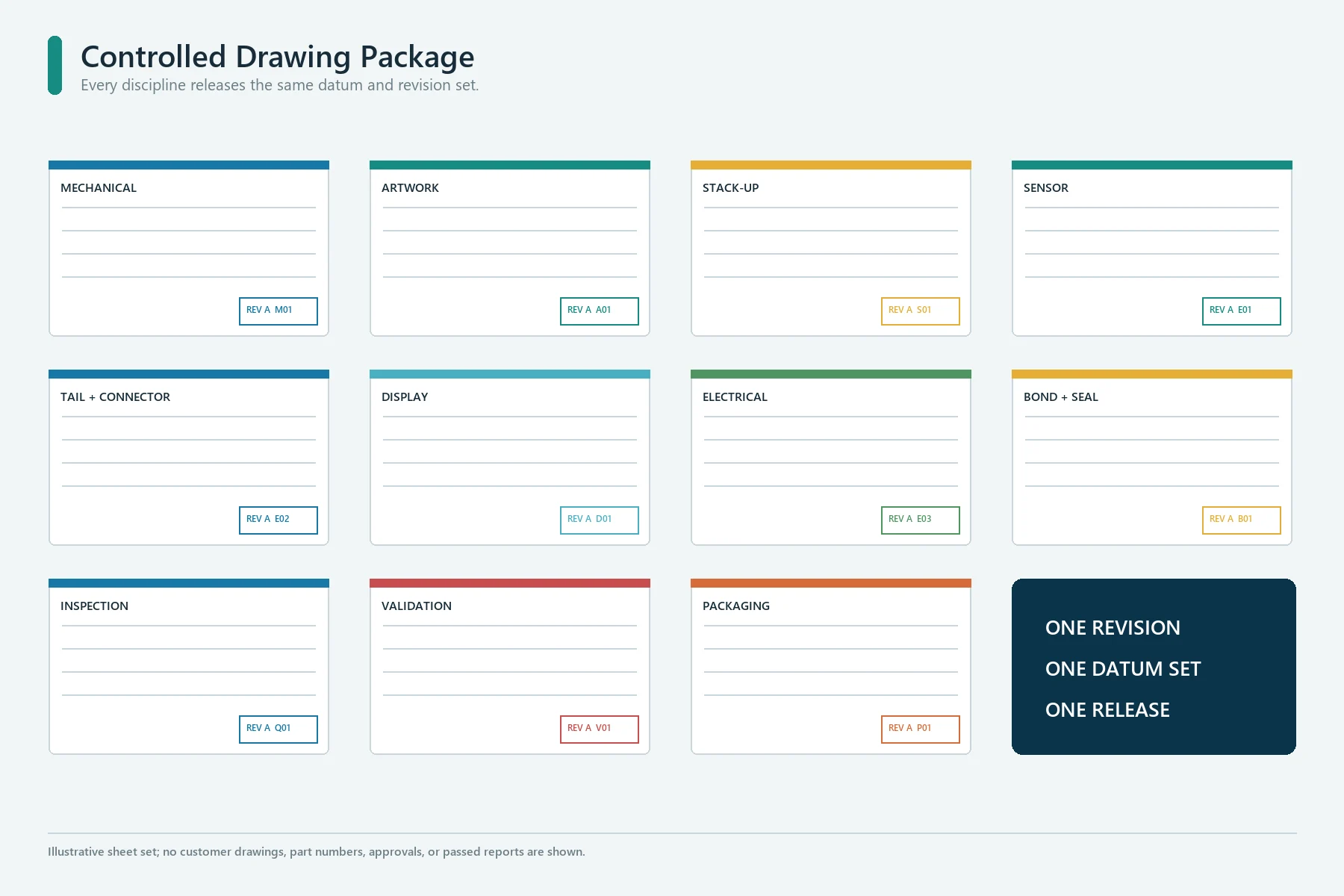
The drawing package is the production contract between disciplines.
| File or sheet | Minimum content |
|---|---|
| Mechanical cover drawing | Outline, thickness, holes, edges, curvature, datums, tolerances, finish |
| Artwork | Colors, layers, windows, dead-front states, icon centers, orientation, revision |
| Stack-up | Cover, print, bond, sensor, shield, display, gasket, enclosure interfaces |
| Sensor drawing | Architecture, electrodes, routing, origin, active area, keepouts, controller mapping |
| Tail and connector | Outline, pinout, contact side, stiffener, bend and keepout zones, mating part |
| Display/interface drawing | View area, active area, border, orientation, mounting, noise/ground assumptions |
| Electrical boundary | Controller, supply, host interface, ground, shield, programming, diagnostics |
| Bonding/sealing drawing | Adhesive/gasket geometry, surface, liner, tail exit, assembly sequence |
| Inspection plan | Dimensions, cosmetics, registration, continuity, lighting, touch function |
| Validation plan | States, samples, repetitions, environment, expected response, evidence |
| Packaging and handling | Protective films, liners, trays, bend protection, labels, ESD controls if applicable |
Use PDF for controlled viewing and native CAD/artwork formats for production. Record software versions and fonts where artwork output can change. A screenshot or flattened image is not enough to manufacture registered print and sensor layers.
Manage the Tolerance Stack Across Layers
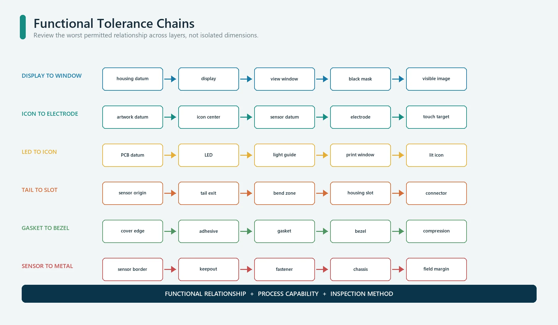
Tolerance review should answer one question: can the worst permitted combination still assemble, look correct, and meet touch behavior?
Housing datum
  + enclosure opening and recess
  + adhesive or gasket location
  + cover outline and print registration
  + sensor registration
  + display position
  + tail exit and connector route
  = installed visual, mechanical, and sensing relationship
Review functional chains, not isolated dimensions
Important chains include:
- display image to clear window and black mask;
- icon center to electrode center;
- electrode border to metal bezel or ground;
- LED center to icon and diffuser;
- adhesive border to window, sensor, and panel edge;
- tail exit to enclosure slot and bend path;
- connector to mating PCB and service access;
- cover flatness plus adhesive variation plus sensor support;
- gasket compression plus bezel and housing tolerances.
Do not assign a tight tolerance because it looks professional. Assign it because the functional chain, process capability, inspection method, and cost justify it. Mark critical-to-function dimensions so inspection does not treat every cosmetic and electrical feature as equal.
Prototype in Stages Instead of Approving One Pretty Sample
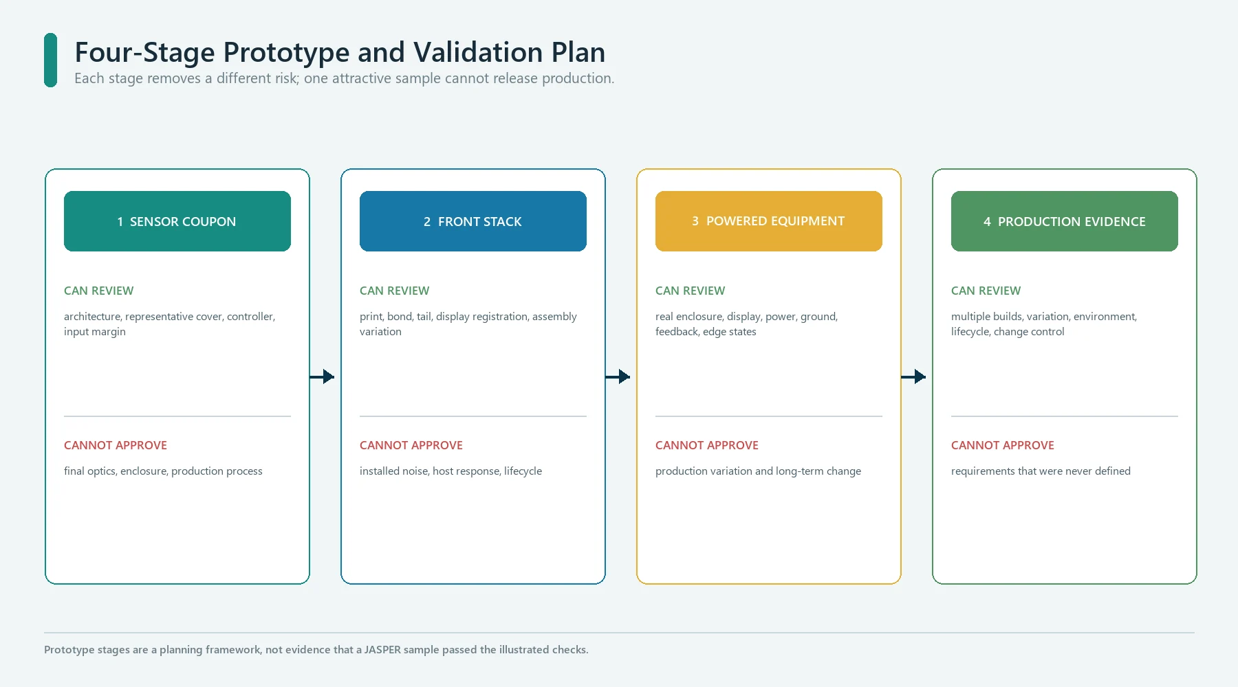
JASPER’s current prototyping page is mainly membrane-switch focused, but its core principle applies: a prototype is a risk-reduction tool, not only a visual sample. Exact PCAP prototype and test capability must be confirmed for the project.
Stage 1: architecture and sensor coupon
Use representative cover material, controller, sensor geometry, ground, and known input objects to test whether the concept has useful margin. This stage does not approve final optics, enclosure, water behavior, or production assembly.
Stage 2: production-intent front stack
Add real print, bond, sensor carrier, tail, connector, lighting, and display relationship. Check registration, stack variation, visual quality, and touch behavior. A hand-built sample may still differ from the production process, so record those differences.
Stage 3: installed powered equipment
Install the panel in the real enclosure with the production display, power, ground, metal, cables, host firmware, feedback, and environmental states. Exercise center, edge, corner, adjacent, rapid, held, invalid, water, glove, cleaning, startup, and recovery cases.
Stage 4: production and lifecycle evidence
Test multiple builds, allowed material and process variation, repeated assembly, environment, aging, cleaning, cycling, transport, and service actions required by the project. Freeze drawings, controller configuration, firmware, inspection, and change control only after the evidence is reviewed.
Create a Validation and Sample-Approval Matrix
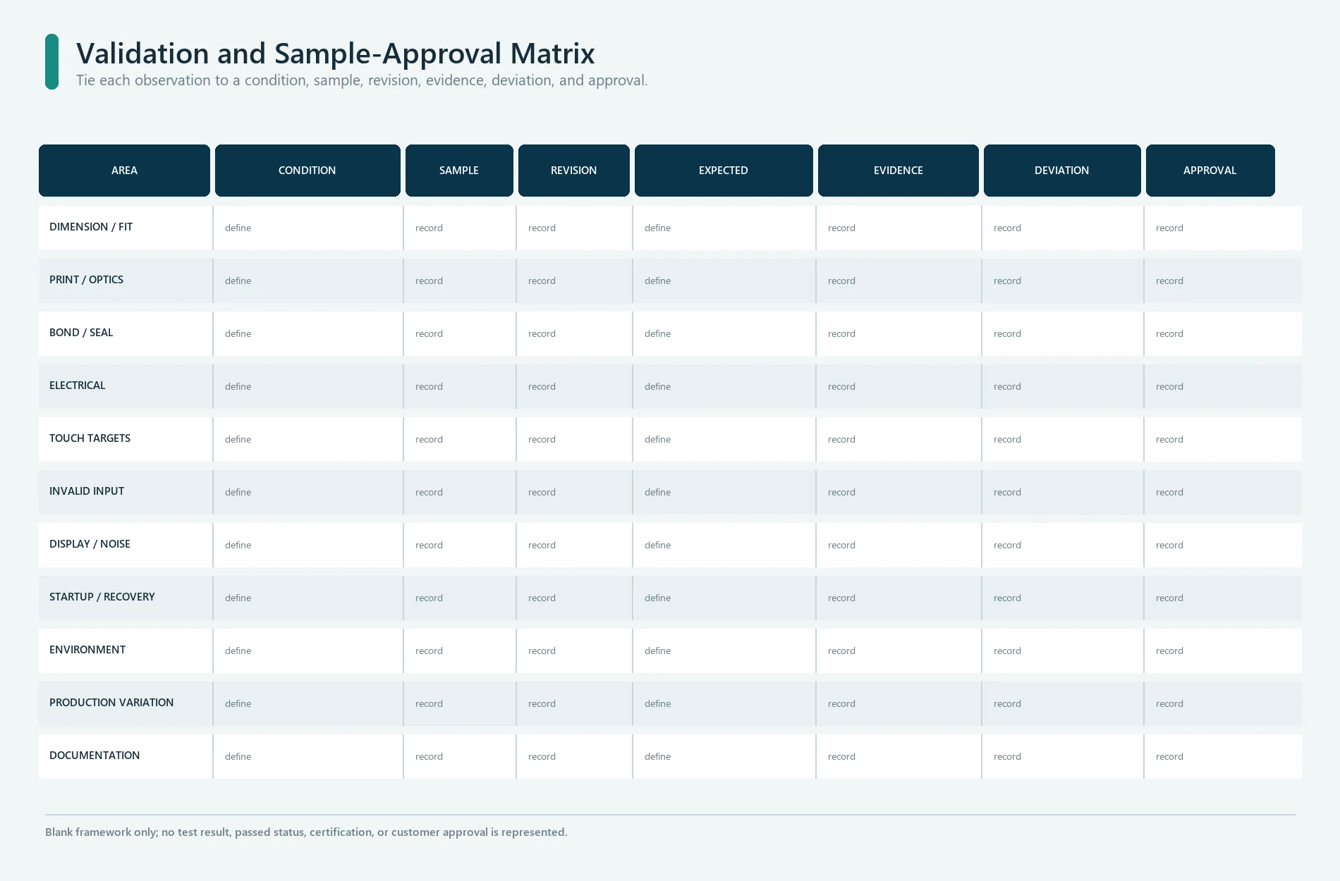
Separate appearance, mechanics, electrical integrity, sensing, host behavior, environment, and documentation.
| Area | Example condition | Expected evidence |
|---|---|---|
| Dimensions and fit | Cover, window, tail, connector, enclosure | Measured values tied to drawing revision |
| Printing and optics | Lit/unlit icons, window, mask, color, defects | Approved master and inspection record |
| Bond and seal | Surface preparation, liner, bubbles, gasket, tail exit | Assembly record and defined boundary test |
| Electrical | Continuity, pinout, shorts, supply, communication | Test result and fixture revision |
| Touch | Every target, edge/corner, adjacent, hold, rapid sequence | Raw/processed data and accepted behavior |
| Invalid input | Palm, sleeve, tool, water state, unintended region | Rejected, disabled, or fault response |
| Display/noise | Display states, charging, radio, motors, LEDs | Stable behavior in worst approved modes |
| Startup/recovery | Power cycle, reset, wet startup, disconnection | Defined safe state and recovery result |
| Environment | Approved temperature, humidity, cleaning, UV, vibration | Project-specific test record |
| Production variation | Multiple covers, sensors, bonds, controllers, assemblies | Distribution, limits, and approval decision |
| Documentation | Drawing, BOM, firmware, configuration, test plan | Matching revision set |
Avoid sample approved without conditions. The approval should identify sample
IDs, drawing and artwork revisions, controller and firmware versions, display,
enclosure, test states, deviations, and required production changes.
Lock Manufacturing and Engineering Changes
A seemingly equivalent substitution can affect sensing, optics, bonding, or noise.
Control changes to:
- cover supplier, material, coating, thickness, strengthening, and flatness;
- ink system, print order, opacity, metallic content, and cure;
- adhesive, gasket, liner, thickness, and die-cut geometry;
- sensor substrate, conductor, trace geometry, sheet or layer properties;
- PCB/FPC stack, copper, solder mask, shield, and connector;
- controller device, firmware, configuration, programming, and test fixture;
- display, backlight, cable, power supply, and host PCB;
- enclosure, bezel, metal, fastener, grounding, and assembly process;
- cleaning product, glove, environment, or required behavior;
- packaging, protective film, storage, and transport.
The capacitive touch panel manufacturing page describes JASPER’s current overlay, sensor, PCB/FPC, lighting, adhesive, connector, inspection, and assembly-review scope. Project-specific controller, firmware, process capability, test equipment, certification, and production limits still require written confirmation.
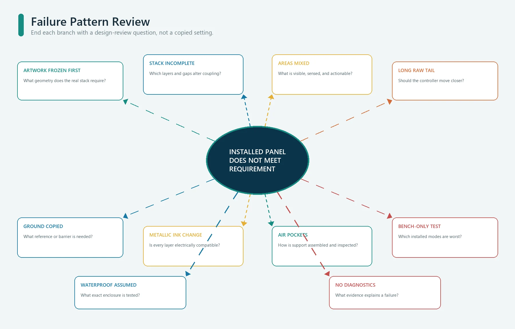
Common Design Failures and the Better Review Question
| Failure pattern | Why it happens | Better question |
|---|---|---|
| Artwork is frozen before sensor review | Icons, windows, LEDs, and bezels consume the sensing space | What geometry does the real stack and controller require? |
| Bench sample passes, installed unit fails | Display, metal, power, ground, and cables changed | Which installed modes create the worst signal and noise? |
| Cover is specified by substrate only | Print, adhesive, gap, coating, and variation were omitted | What is the complete dielectric stack? |
| Touch target and active area are confused | Display, sensor, and UI drawings use different boundaries | Which area is visible, sensed, and actionable? |
| Long raw-sensor tail is added late | Connector and cable parasitics were ignored | Should the controller move closer to the sensor? |
| Ground or shield is copied from another design | Electric-field and controller differences were ignored | What reference, shield, and noise problem must be solved? |
| Metallic print changes after approval | Decorative ink was treated as cosmetic only | Is every layer above the sensor electrically compatible? |
| Air pockets vary across units | Bond support and flatness were not controlled | How is the sensor-to-cover path assembled and inspected? |
| Waterproof is claimed from a flat face | Tail, edge, gasket, and enclosure boundary were omitted | What exact enclosure is tested to which target? |
| Glove or wet use is one checkbox | Real states and recovery behavior were not defined | Which inputs must be accepted, rejected, disabled, or reported? |
| No raw-data or diagnostic access exists | Only final button events were exposed | What evidence will explain failures during validation and production? |
| One sample becomes the golden unit | Variation and change control were not tested | Which builds and limits define acceptable production? |
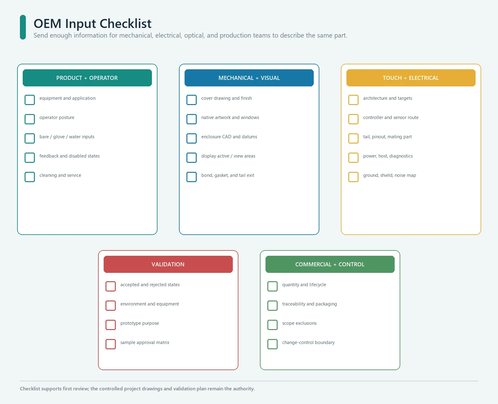
OEM Input Checklist
Send enough information to let mechanical, electrical, optical, and production reviews describe the same part.
Product and operator
- equipment and application;
- operator posture and viewing distance;
- bare finger, glove, stylus, water, and invalid inputs;
- required feedback;
- safety-related or disabled states;
- cleaning and service method.
Mechanical and visual
- cover outline, material concept, thickness, finish, edges, and mounting;
- artwork, colors, icons, display windows, dead-front and backlit states;
- enclosure CAD, bezel, recess, metal, fasteners, and datums;
- display drawing, orientation, view area, and active area;
- adhesive, gasket, surface, tail exit, and assembly sequence.
Touch and electrical
- discrete keys, slider, wheel, touchpad, coordinate area, or multi-touch;
- touch target and active-area geometry;
- controller candidate and sensing architecture;
- electrode carrier and routing concept;
- tail, connector, pinout, mating part, and cable route;
- supply, host interface, firmware ownership, programming, diagnostics;
- ground, shield, chassis, display, noise sources, EMC/ESD target.
Validation and commercial
- required accepted, rejected, lockout, recovery, and fault behavior;
- environment and applicable equipment standards;
- prototype purpose and approval matrix;
- samples, repetitions, production variation, and lifecycle conditions;
- critical dimensions and inspection method;
- annual quantity, service life, packaging, and traceability;
- scope exclusions and customer-supplied parts.
The current JASPER capacitive touch design checklist PDF can support the first file review. The controlled project drawing and validation plan remain the authority.
Stop Conditions Before Tooling or Production Release
Stop the release when any of the following remains unclear:
- The purchased assembly boundary is not written.
- Cover, print, adhesive, gap, and sensor are not one controlled stack.
- Display view area, touch active area, and user targets are mixed.
- Sensor architecture or controller is still an unnamed future decision.
- Tail, connector, ground, shield, metal, or display-noise data is missing.
- Artwork and sensor files do not share datums and revision control.
- Water, glove, cleaning, invalid input, feedback, and recovery states are vague.
- The seal is claimed without the enclosure, tail exit, and test boundary.
- The prototype is not representative of the approved production stack.
- Sample approval lacks IDs, revisions, conditions, evidence, or deviations.
- Production substitutions can occur without touch and optical review.
- JASPER and buyer responsibilities differ between the quote and the drawings.
Frequently Asked Questions
What files should I send for a custom capacitive touch panel?
Send the cover and enclosure drawing, native artwork, display outline, touch targets, sensor or controller constraints, stack-up, tail and connector details, ground/noise information, environment, validation states, and expected quantity. A sketch can start a discussion, but production needs controlled files.
Can capacitive touch work through glass, acrylic, or polycarbonate?
Yes, when the controller, electrode geometry, complete dielectric stack, input object, ground, noise, and installed validation support it. Do not select an electrode from cover material alone.
Does every capacitive panel require a transparent ITO sensor?
No. Discrete buttons, sliders, and wheels can use opaque PCB, FPC, or printed sensor constructions behind graphics. A display coordinate area may require a transparent sensor. The optical and sensing architecture decides.
Should the touch controller be on the panel or the main PCB?
Either can be valid. A remote controller may expose raw sensor lines to a long tail and connector. A local controller shortens those paths but adds power, firmware, programming, communication, and lifecycle responsibilities to the panel. Compare the complete system.
Is optical bonding required?
Not for every design. Perimeter bonding, full-surface bonding, an intentional display air gap, or another construction can be appropriate. The choice affects optics, sensing, stress, sealing, service, and process control and should be validated in the actual stack.
When should the controller be selected?
Before the sensor and tail are released. The controller affects sensing mode, electrode support, channel mapping, layout, shielding, diagnostics, tuning, host interface, and test access.
Can a flat capacitive panel be called waterproof?
Not from appearance alone. Waterproof or IP performance depends on the exact enclosure, cover bond, gasket, edges, openings, tail exit, connector path, and test target. The tested boundary must be named.
Is one approved sample enough for production?
No. One unit can approve appearance or demonstrate a concept, but production release should also address allowed material, process, assembly, controller, firmware, environment, and unit-to-unit variation.
What should be included in touch-function acceptance?
Include every required target, edge and corner use, adjacent input, rapid and held touch, startup, reset, display and power modes, approved gloves, water and cleaning states, invalid contacts, feedback, lockout, recovery, faults, and production variation.
Submit the Panel Drawing and System Boundary
Send the cover and enclosure files, display outline, touch targets, controller plan, stack-up, tail and connector, ground/noise map, environment, and approval matrix through the JASPER RFQ form. The first review should decide what JASPER supplies, what the buyer supplies, which risks need a prototype, and which evidence must exist before tooling or production release.
Sources
- JASPER Electronics, “Custom Capacitive Touch Panels and Switches for Sealed OEM Interfaces.” https://www.jasperele.com/products/capacitive-touch-panels/
- JASPER Electronics, “Capacitive Touch Switch Guide.” https://www.jasperele.com/resources/capacitive-touch-switch-guide/
- JASPER Electronics, “Capacitive Touch Switch Manufacturer.” https://www.jasperele.com/manufacturing/capacitive-touch-switch-manufacturer/
- JASPER Electronics, “Capacitive Touch Control Panel for a Sealed Interface.” https://www.jasperele.com/case-studies/capacitive-touch-control-panel/
- JASPER Electronics, “Membrane Switch Prototyping.” https://www.jasperele.com/capabilities/prototyping/
- Microchip Technology, “Capacitive Touch Sensor Design Guide AN2934.” https://onlinedocs.microchip.com/oxy/GUID-A8A0085D-58D1-4E41-A07D-B93BFDE11AFE-en-US-4/GUID-80CF1688-09E6-46D2-B2C6-44743EA74277.html
- Texas Instruments, “CapTIvate Technology Guide: Design Guide.” https://software-dl.ti.com/msp430/msp430_public_sw/mcu/msp430/CapTIvate_Design_Center/1_83_00_08/exports/docs/users_guide/html/CapTIvate_Technology_Guide_html/markdown/ch_design_guide.html
- International Organization for Standardization, “ISO 9241-210:2019, Ergonomics of human-system interaction – Part 210: Human-centred design for interactive systems.” https://www.iso.org/standard/77520.html
- International Electrotechnical Commission, “IEC 60529:1989+AMD1:1999+AMD2:2013 CSV, Degrees of protection provided by enclosures (IP Code).” https://webstore.iec.ch/en/publication/2452