
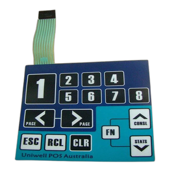
Membrane switch design mistakes are layout, material, tolerance, and circuit errors locked into a drawing that, once steel-rule dies or screen-printing screens are cut, cost USD 500–15,000 and 2–6 weeks to undo — most of them visible in a 30-minute pre-tooling drawing review.
- 1. Why these mistakes get expensive after tooling
- 2. The 10 design mistakes that get locked in at tooling
- 2.1 Insufficient button size and spacing for gloved or wet operation
- 2.2 Wrong overlay material for the operating environment
- 2.3 Tolerances tighter than the steel-rule die can hold
- 2.4 Inadequate perimeter seal width for the claimed IP rating
- 2.5 Tactile dome chosen without considering ambient temperature
- 2.6 Trace spacing and silver-migration risk ignored
- 2.7 Keep-out zones around LEDs, domes, and windows violated
- 2.8 Tail routing and pin-out fixed before the manufacturer reviews it
- 2.9 Adhesive system mismatched to the mounting substrate
- 2.10 ESD and EMI shielding deferred to “later”
- 3. The pre-tooling drawing-review table
- 4. Standards and specifications to reference in the drawing
1. Why these mistakes get expensive after tooling
A membrane switch looks like a printed sticker. The economics behave like a small injection-moulded part. Once a supplier cuts the steel-rule die, burns the silver-ink screens, and machines the embossing tool, those three items are committed dollars and committed weeks. A change at that point is not a graphic revision — it is new tooling.
Vendor design guides from Cubbison, Epec, and General Label converge on the same cost ladder. A pre-tooling graphic update is USD 200–500 and one to two weeks. A post-tooling button-layout change rebuilds the die at USD 500–1,500 and two to three weeks. A material or circuit redesign rebuilds dies, screens, and embossing together: USD 2,500–15,000 and four to six weeks, longer if a medical-device file at ISO 13485 must be re-validated. Lead times land at 8–12 weeks for a clean design, 16+ weeks when regulatory review re-opens.
The global membrane switch market reached roughly USD 1.16 billion in 2024 and is forecast at 5.1% CAGR through 2030 (Grand View Research, 2024). A 4-week re-tooling delay on a medical infusion-pump programme or a Tier-1 automotive console shifts production-launch dates and triggers penalties that dwarf the tooling line.
The fix is the part of the project nobody bills for: a structured pre-tooling drawing review. Most of the costly mistakes below take 30 minutes to catch on paper and weeks to catch in steel.
2. The 10 design mistakes that get locked in at tooling
2.1 Insufficient button size and spacing for gloved or wet operation
The most common ergonomic mistake is sizing buttons to the look of the overlay rather than to the operator’s hand. For ungloved fingertip use, 12 mm centre-to-centre is workable. For nitrile-gloved medical use, push to 15 mm. For thick industrial gloves, 19 mm. Wet operation amplifies the problem because surface tension makes a finger slip — adding 1 mm of tactile emboss around each key rescues legibility under spray. Catch-it-now signal: the drawing lists button pitch in mm and the operator persona.
2.2 Wrong overlay material for the operating environment
Polycarbonate prints sharply and embosses cleanly, which is why it dominates first-pass designs. It is also the worst overlay choice for sustained UV, sustained chemical contact, or above 1 million actuation cycles. Polyester (PET) survives 1,000,000+ cycles in published life testing; uncoated polycarbonate wears before 100,000 cycles in the same protocol (Cubbison design notes). For UV-heavy outdoor use, specify autotextured polyester with a fluoropolymer hardcoat. Catch-it-now signal: the drawing names the polymer (PET vs PC), the surface treatment, and the hardcoat.
2.3 Tolerances tighter than the steel-rule die can hold
Steel-rule dies — the standard tool for cutting the overlay and underlying layers — hold roughly ±0.010 in (±0.25 mm) on critical dimensions per General Label’s design specification. Drawings calling for ±0.005 in (±0.13 mm) on a window cutout force a switch to hard tooling or laser cutting, with a corresponding 25–60% cost premium and longer lead time. Circuit-layer features are typically inset 0.015 in (0.38 mm) from overlay edges to absorb the tolerance stack. Catch-it-now signal: the drawing’s title-block tolerance is ±0.25 mm or looser unless a feature is explicitly flagged as needing a tighter process.
2.4 Inadequate perimeter seal width for the claimed IP rating
A drawing that calls out IP65 sealing while showing a 1.5 mm sealed border around a window cutout has a contradiction the supplier will catch in week 3 of tooling. For IP54 splash resistance, a 2 mm continuous adhesive border around all openings is the practical minimum; for IP65 jet resistance, 3 mm is closer to safe; for IP67 immersion, 4 mm with a gasket layer is typical. IEC 60529 defines the rating itself but not the design — that is on the drawing. Catch-it-now signal: measure the sealed border on every cutout in CAD; flag any below the IP-rating threshold above.
2.5 Tactile dome chosen without considering ambient temperature
Polyester (poly) domes are silent, low-cost, and lose tactile response above roughly 50 °C / 122 °F as the polymer relaxes (Reliatrace design guide). They are wrong for outdoor enclosures in desert climates, near heat-producing electronics, or in autoclave-adjacent medical equipment. Stainless-steel snap domes hold tactile feel up to 85 °C and beyond and offer a sharper click, at higher unit cost. A 0.015–0.020 in backing layer behind a metal dome prevents inversion during assembly. Catch-it-now signal: the drawing lists dome material, actuation force in newtons (typically 3–8 N), and the maximum operating temperature.
2.6 Trace spacing and silver-migration risk ignored
Screen-printed silver ink is not a copper trace. Under humidity and applied voltage, silver ions migrate between traces and form dendrites that short the circuit. IPC-2221A spacing rules for printed conductors must be derated for silver — a useful rule of thumb is to double the IPC-2221A minimum gap for silver traces in humid environments and apply a dielectric overcoat on critical spans. Catch-it-now signal: the circuit drawing shows trace width and gap explicitly, lists the conductive ink, and references IPC-2221A or names the dielectric overcoat ink.
2.7 Keep-out zones around LEDs, domes, and windows violated
A keep-out is a region of the circuit layer where no traces may pass — typically a 1.5–2 mm halo around every LED pad, every dome footprint, every die-cut window, and every embossed button perimeter. A trace running under a dome footprint will short on the first actuation; a trace under an LED pad will lift during reflow or hot-bar bonding. Catch-it-now signal: the circuit drawing shows keep-out polygons overlaid on trace routing; visually trace each LED pad and dome to verify clearance.
2.8 Tail routing and pin-out fixed before the manufacturer reviews it
Tail pin-out — the order in which signals exit the flex tail — affects whether the trace routing can be done in one circuit layer or needs jumpers. A drawing that locks pin 1 at one corner because that is what the PCB connector expects often forces an avoidable jumper bridge on the membrane, which raises cost and lowers yield. The manufacturer’s process engineer can usually reorder pin assignments to single-layer-routable in 10 minutes, then the PCB layout adapts. Catch-it-now signal: treat the pin-out as negotiable in the drawing; ask the supplier for a one-layer-routable alternative before freezing the PCB.
2.9 Adhesive system mismatched to the mounting substrate
The rear adhesive is not a default. 3M 467MP holds on smooth painted metal; on powder-coated textured surfaces, 3M 9495LE or VHB-class adhesives are needed. On low-surface-energy plastics (PP, PE), an LSE-rated adhesive plus a primer is the only configuration that survives thermal cycling. Acrylic adhesives have better peel than shear, so a switch under continuous shear from thermal-expansion mismatch can delaminate even when peel-tested fine. Catch-it-now signal: the drawing names the substrate, the surface finish, and the specific adhesive part number — not a generic “acrylic adhesive”.
2.10 ESD and EMI shielding deferred to “later”
A keypad on a medical device, a factory-floor HMI, or an aerospace cockpit must usually pass IEC 61000-4-2 ESD and IEC 61000-4-3 radiated-immunity testing. Adding a printed silver shield, a copper-foil grounded shield, or an indium-tin-oxide shield after the rest of the stack is fixed forces a circuit redesign — the shield needs keep-outs, a ground tail, and dielectric isolation. An ungrounded shield is worse than no shield because it re-radiates. Catch-it-now signal: the drawing states ESD/EMI requirements up front; if any apply, the shield layer is in the stack from revision A.
3. The pre-tooling drawing-review table
Review these items with the supplier on a 30-minute call before any die or screen is cut.
| Mistake | Detection stage | Cost if caught at tooling release | Cost if caught at production | Catch-it-now signal on the drawing |
|---|---|---|---|---|
| Button pitch wrong for gloved use | Drawing review | USD 0 (graphic edit) | USD 800–1,500 (new die) | Pitch dimension + operator persona stated |
| Overlay polymer wrong | Drawing review | USD 200 (new screen file) | USD 2,500+ (full rebuild) | PET vs PC + surface + hardcoat stated |
| Tolerance tighter than die capability | Drawing review | USD 0 (loosen tolerance) | USD 1,500–4,000 (hard tooling) | Title-block at ±0.25 mm |
| Perimeter seal too thin for IP rating | Drawing review | USD 200 (cutout adjust) | USD 1,200 (new die + retest) | Seal width ≥ IP-rating minimum |
| Poly dome above 50 °C ambient | Drawing review | USD 0 (swap to metal dome) | USD 1,500–3,000 (new dome set + rework) | Dome material + max temp on drawing |
| Trace spacing too tight for silver ink | Drawing review | USD 100 (re-route) | USD 2,000+ (new screen) | Trace width / gap + IPC-2221A reference |
| Keep-out violation under LED or dome | Drawing review | USD 100 (re-route) | USD 2,500 (new circuit screen) | Keep-out polygons in CAD |
| Pin-out forces a jumper | Drawing review | USD 0 (re-order pins) | USD 1,800 (jumper bridge + yield loss) | Pin-out marked “negotiable” |
| Wrong adhesive for substrate | Drawing review | USD 50 (spec change) | USD 4,000+ (field delamination) | Substrate + adhesive part number named |
| ESD shield added after stack-up freeze | Drawing review | USD 200 (add layer) | USD 8,000–15,000 (full redesign) | ESD/EMI requirement on drawing rev A |
The right-hand column is the entire content of a useful pre-tooling review. If every row has a clean answer, the drawing is releasable.
4. Standards and specifications to reference in the drawing
Drawings that name the standards they comply with shorten the supplier’s RFQ-response cycle and remove a category of post-tooling argument. The six standards below cover most non-aerospace, non-defence programmes.
| Standard | What it specifies | What the drawing should reference |
|---|---|---|
| IPC-2221A | Generic circuit design — trace width and spacing vs voltage | Minimum trace and gap per applied voltage, derated for silver ink |
| IPC-A-600 | Acceptability of printed boards including flex | Class 2 commercial vs Class 3 high-reliability acceptance criteria |
| IEC 60529 | IP rating definitions (IP54 / IP65 / IP67) | The exact IP rating the assembled switch must hold, with test method |
| UL 746C | Polymer material flammability, RTI, weatherability | UL recognition file number for the overlay polymer |
| ASTM D3359 | Cross-hatch tape adhesion test | Required pass class (4B or 5B) for the graphic overlay |
| ISO 13485 | Medical-device quality management system | Required when the end product is a regulated medical device |
A drawing that cites these standards, with target classes filled in, gives the supplier’s engineering team a clean specification to quote against. A drawing that leaves the standards unstated invites either a higher quote (the supplier bids worst-case) or an under-spec build that fails compliance testing.
5. Frequently Asked Questions
What is the most expensive membrane switch design mistake to fix after tooling?
Deferring ESD or EMI shielding. Adding a shield layer after the rest of the stack-up is frozen forces a circuit redesign, new screens, new dielectric layers, and re-validation. Published vendor cost notes put the rework at USD 8,000–15,000 and 4–6 weeks. A shield-layer line on revision A of the drawing prevents the entire chain.
What should an engineer check on a membrane switch drawing before sending it to the supplier?
Ten items: button pitch and operator persona; overlay polymer, surface, hardcoat; title-block tolerance at ±0.25 mm or looser; perimeter seal width matched to IP rating; dome material vs operating temperature; trace spacing for silver ink; keep-out zones around LEDs and domes; tail pin-out flagged negotiable; named adhesive matched to substrate; ESD or EMI requirements on revision A.
Why is ±0.25 mm the typical lower limit on membrane switch tolerances?
Steel-rule dies, the standard tool for cutting overlay, spacer, and circuit layers, hold roughly ±0.010 in (±0.25 mm) on critical dimensions per General-Label specifications. Tighter than that requires hard tooling or laser cutting, adding cost and lead time. Drawings should specify ±0.25 mm unless a feature genuinely needs a tighter process.
When should an engineer choose polyester instead of polycarbonate for the overlay?
When the switch will see more than 100,000 actuations, sustained UV, or repeated chemical contact. Polyester survives 1,000,000+ cycles in published life testing; uncoated polycarbonate wears before 100,000 cycles. For sustained chemical exposure, autotextured polyester with a fluoropolymer hardcoat is the durable choice. Polycarbonate stays appropriate for indoor, low-cycle, low-chemical consumer applications.
How much perimeter seal width is needed for an IP65 membrane switch?
Roughly 3 mm of continuous adhesive border around every cutout and window is the practical IP65 minimum. IP54 splash resistance works at 2 mm; IP67 immersion typically needs 4 mm plus a gasket layer. IEC 60529 defines the rating but not the seal geometry — the geometry must be designed into the drawing and verified during the pre-tooling review.
Why do poly domes fail above 50 °C and metal domes do not?
Polyester domes rely on the elastic deformation of the polymer to snap and reset. Above roughly 50 °C / 122 °F, polyester relaxes and the dome loses its tactile click and reset force. Stainless-steel snap domes rely on the elastic deformation of metal, which is stable to 85 °C and well beyond — at higher unit cost and slightly louder click.
Should the tail pin-out be fixed in the drawing or left to the manufacturer?
Mark the tail pin-out as negotiable on the first drawing revision. The supplier’s process engineer can usually re-order pin assignments to keep the circuit routable in one layer, which lowers cost and raises yield. PCB layout can then adapt to the optimised pin-out, rather than the membrane absorbing avoidable jumper bridges.
How early in the device design process should the membrane switch supplier be involved?
At the industrial-design stage, before the enclosure CAD is frozen. Late involvement is the failure mode behind most pre-tooling rework: the supplier finds tolerance, seal-width, or pin-out problems the OEM team did not flag. A 30-minute call at concept stage and a second at drawing release prevents most of the mistakes above.
This explainer was authored by Jasper Electronics, a membrane switch and keypad manufacturer based in Shenzhen. The mistakes above apply to any supplier’s tooling stage; readers are welcome to verify the standards cited against IPC, IEC, UL, and ASTM source documents directly.
Ready to Start Your Project?
Tell us about your membrane switch, keypad, or graphic overlay requirements. Our engineering team will review your specifications and provide a detailed quote.


Related engineering paths
Continue with product specifications, supplier checks, or a project RFQ.