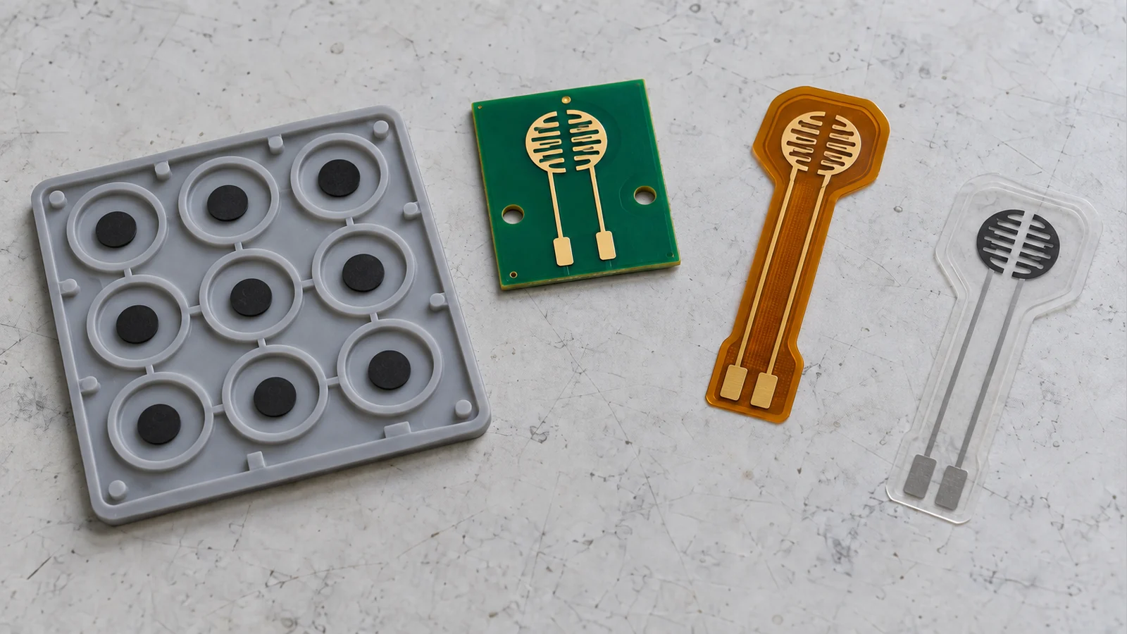
For a silicone keypad assembly, choose the circuit carrier from the complete contact, support, routing, and assembly system. A rigid PCB is usually easiest when the key field needs a stable reaction surface and the same carrier also holds LEDs, resistors, connectors, or other electronics. A copper FPC is useful when the circuit must fold through a compact enclosure or reach another board, but the key, component, and connector zones may still need local support. A screen-printed circuit on PET or another compatible film can create a thin flexible contact layer, but its conductor, contact coating, backing, component attachment, and termination must be defined as one material/process stack.
JASPER’s current silicone keypad assemblies page already treats the molded keypad, circuit, LEDs, connector, spacer, housing interface, and test boundary as one system. The decision here is narrower: which circuit construction should sit under the silicone keypad, and what interfaces must be controlled around it?
- Define the Three Circuit Choices First
- 1. List Electrical and Mechanical Requirements
- Circuit Carrier vs Silicone Keypad Interface
- 2. Compare Routing and Component Integration
- Rigid PCB
- FPC
- Printed Circuit on Film
- 3. Review Support, Flexing and Tail Routing
- 4. Coordinate Contact Surfaces and Connectors
- 5. Compare Tooling and Assembly Scope
- Illustrative Cross-Sections and Supply BOMs
- A. Silicone Keypad + Rigid PCB
- B. Silicone Keypad + Supported FPC
- C. Silicone Keypad + Printed-Film Circuit + Support
- How to Validate the Selected Construction
- What Should an OEM Send?
- Discuss a Hybrid Keypad Assembly
Define the Three Circuit Choices First
In this article:
- Rigid PCB means etched copper on a rigid board that can provide electrical routing and, when correctly mounted, a stable reaction surface below the key field.
- FPC means an etched-copper flexible printed circuit, typically on polyimide with coverlay and local stiffeners where needed. FPC is a circuit technology, not automatically a membrane switch.
- Printed circuit means a flexible circuit formed by screen-printing conductive ink, commonly silver and/or carbon, on a compatible film such as PET. It is not the same construction as a copper FPC.
If an RFQ only says “flex circuit,” identify which construction is actually intended before discussing price or tooling.
1. List Electrical and Mechanical Requirements
Start with the installed keypad, not the preferred fabrication method.
Define the electrical architecture: key matrix or discrete switches, sensing threshold, LEDs or other components, connector and pinout, and where final continuity or resistance will be measured. Then define the mechanical stack: key centers, force and travel, carbon pill or other actuator, support below the contact area, enclosure bosses and hard stops, tail route, fixed or repeated bends, and the sealing interface.
This is important because a silicone contact does not switch in isolation. JASPER’s current carbon-pill resistance guide treats pad geometry and finish, support, force, overtravel, contamination, and the measurement circuit as one installed interface.
Circuit Carrier vs Silicone Keypad Interface
| Design question | Rigid PCB | Copper FPC | Screen-printed flexible circuit |
|---|---|---|---|
| Key-field support | Can provide the reaction surface if the board is correctly mounted | Often needs local support under key/contact zones | Usually needs a backer, housing land, or other support |
| Routing | Best for planar layouts | Strong for folds, narrow routes, and remote connections | Strong for thin planar/tail layouts; forming depends on the ink/substrate stack |
| Components | Well suited to conventional soldered electronics | Components are possible, often with stiffened zones and bend keep-outs | Attachment is process-specific; do not assume conventional soldering |
| Contact surface | Specified plated/coated pads | Exposed plated contact features with controlled coverlay opening and support | Printed silver/carbon contact areas with controlled cure and surface condition |
| Connector / tail | Board connector, header, harness, or separate flex | Integral FPC tail can mate with ZIF/FFC or another connector | Integral printed tail is possible when termination is designed for the material system |
| Main assembly risk | Board support, flatness, datum and contact cleanliness | Bend line, stiffener, connector-end and support interactions | Ink/substrate/cure, contact surface, support and termination interactions |
| Typical reason to select | Stable key bed plus electronics integration | 3-D packaging and reduced separate wiring | Very thin printed-film contact architecture |
| Does not prove by itself | IP rating, switch life, or contact reliability | Dynamic-flex life, sealing, or contact stability | Solderability, environmental durability, or contact life |
Do not select the carrier from the last row backward. IEC 60529 defines protection provided by enclosures, so choosing PCB instead of FPC or PET does not by itself establish a higher IP rating.
2. Compare Routing and Component Integration
Rigid PCB
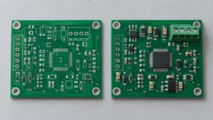
Rigid PCB is a strong default when the keypad can stay planar and the circuit must also carry LEDs, resistors, connectors, protection parts, or controller electronics. It can combine electrical routing and key-field support in one part.
The board is still part of the force path. Review mounting points, unsupported spans, cutouts, component height, vias, mask edges, and contact-pad keep-outs. A poorly supported PCB can still flex under a key.
FPC
The main value of FPC is controlled routing through three-dimensional packaging, not softness under the key. Treat the flex circuit as both an electrical and a mechanical component: review bend design, component mounting, and stiffeners for connector or surface-mount regions together.
Separate four zones in the drawing:
- key/contact zone — control flatness and reaction support;
- component zone — add local stiffening when required;
- bend zone — keep components and stiffener edges away from the intended flex;
- connector zone — match thickness, contact geometry, plating, and stiffener to the chosen connector.
The same FPC can contain all four, but they are not mechanically interchangeable.
Printed Circuit on Film
Printed silver or carbon circuitry can create a thin contact/routing layer, but ‘printed silver’ does not define one universal assembly process. A specifically solderable silver ink and a conductive silver epoxy for bonding surface-mount devices to flexible or rigid printed circuits are different material/process choices. Confirm which route the actual stack supports.
Therefore confirm the actual:
- substrate and temperature limits;
- ink and dielectric system;
- contact overprint or coating;
- solderable versus conductive-adhesive attachment;
- curing process;
- component support and strain relief;
- inspection and repair method.
If those items are not defined, treat the printed circuit as a contact/routing layer rather than assuming it can replace a conventional PCBA.
3. Review Support, Flexing and Tail Routing
A silicone key needs a controlled reaction surface. If the circuit moves downward during a press, part of the key travel is consumed by circuit deflection. That can shift electrical closure, overtravel, force, and contact resistance.
For a rigid PCB, check board thickness, bosses, fasteners, cutouts, and unsupported spans. For FPC, provide a backer, stiffener, or housing support under the key/contact field when required while preserving the intended bend zone. For printed film, explicitly identify the spacer, backer, housing shelf, or other structure that keeps the active contact area flat.
Do not copy one generic FPC bend-radius value into every project. Link bend design to circuit thickness, layer count, and the intended formed state. The supplier’s released construction and application decide the actual limit.
A useful drawing should show both the electrical layer stack and the force path from key top to enclosure.
4. Coordinate Contact Surfaces and Connectors
For carbon-pill designs, specify more than “gold pad,” “copper,” or “silver ink.” Define pad geometry and gap, final contact surface, mask/coverlay relationship, local flatness and support, contamination controls, shared keypad-to-circuit datum, and the installed resistance/continuity test method.
A rigid PCB, exposed FPC contact, and printed-film contact can all be valid candidates, but a change in contact surface or support should be treated as an interface change that may require revalidation.
For connector tails, release the circuit termination and connector as a matched pair. A specific connector drawing may require defined FPC contact geometry and a polyimide stiffener at the connector end. Do not copy dimensions from another part; let the actual connector control exposed length, contact orientation, insertion thickness, plating, and stiffener requirements.
5. Compare Tooling and Assembly Scope
Do not compare only the circuit-layer price. Compare the same supplied boundary.
A rigid PCB may combine support and electronics. An FPC may remove separate wiring but add stiffeners, forming, and connector-end controls. A printed circuit may simplify a thin contact layer but add screens, die cutting, spacers, a rigid backer, or specialized component attachment.
Ask suppliers to quote the same scope:
- loose silicone keymat;
- keypad + contact circuit;
- keypad + circuit + connector;
- keypad + LEDs/components;
- keypad + support/backer/spacer;
- complete tested keypad module.
JASPER’s silicone rubber keypad design guide also recommends defining the supplied boundary and validating the installed system. That makes commercial comparisons meaningful and avoids comparing a bare keymat with a tested HMI module.
Illustrative Cross-Sections and Supply BOMs
The following are illustrative only, not JASPER production records or customer cases.
A. Silicone Keypad + Rigid PCB
key top → silicone web → carbon pill → PCB contact pad → rigid PCB → housing support
Illustrative BOM: molded keymat, specified contact/actuator, PCB or PCBA, connector, optional LEDs/components, spacer/gasket where required, and agreed functional test.
Best fit: planar key field with strong support and substantial electronics integration.
B. Silicone Keypad + Supported FPC
key top → silicone web → contact → FPC contact zone → local stiffener/backer → bend zone → FPC tail
Illustrative BOM: molded keymat, copper/polyimide FPC, local stiffener/backer, exposed/plated contacts, optional qualified components, connector termination, and formed-state/electrical inspection.
Best fit: compact three-dimensional routing where a separate cable or rigid board shape is inconvenient.
C. Silicone Keypad + Printed-Film Circuit + Support
key top → silicone web → contact/actuator → printed contact on film → spacer as required → rigid backer → printed tail
Illustrative BOM: molded keymat, printed conductive circuit, dielectric/spacer, rigid support, compatible termination, optional components only where the attachment process is qualified, and supported-assembly electrical test.
Best fit: thin printed-film contact architecture with a deliberately separate support/electronics boundary.
How to Validate the Selected Construction
- Confirm keypad, circuit, support, tail, connector, and enclosure datums.
- Measure force and travel on the production-intent support.
- Verify first electrical closure, stable closed state, release, and intermittency at defined sense points.
- Inspect the contact area for contamination, mask/coverlay steps, wrinkles, poor overlap, or board/film deflection.
- Check bend location, connector retention, clearance, and installation stress.
- Run project-specific environment and lifecycle tests on the complete stack.
- Repeat affected validation after changes to pad finish, ink, stiffener, connector, support, adhesive, or circuit revision.
What Should an OEM Send?
Send the keypad and enclosure drawings, key force/travel targets, contact method, circuit schematic or matrix, proposed PCB/FPC/printed-circuit data, LED/component list, connector part number, tail route, sealing/environment requirements, test expectations, prototype and production quantities, and the desired supply boundary. Unknown items can be marked TBD.
Discuss a Hybrid Keypad Assembly
If the project is between rigid PCB, copper FPC, and printed flexible circuit, send the keypad layout, enclosure section, circuit requirements, connector plan, quantities, and remaining TBD items. The useful decision is not only the carrier name; it is the combined support, contact surface, routing, termination, and test boundary.
Request a keypad engineering review
Frequently Asked Questions
Is an FPC the same thing as a membrane switch?
No. FPC is a flexible circuit technology. It can be used under a silicone keypad, inside a membrane switch, as an interconnect, or in another assembly.
Does a rigid PCB automatically give a silicone keypad a higher IP rating?
No. The final result depends on the enclosure, keypad sealing features, gaskets, fasteners, penetrations, tolerances, and validated test configuration.
Can SMT components be mounted on FPC?
Yes, when the flex construction, component mass, solder process, local support, and bend location are designed for it. Stiffeners are commonly used in component and connector regions.
Can components be soldered directly to a printed silver circuit?
Sometimes, but not universally. Confirm the exact ink, film, cure, pad finish, attachment process, and reliability plan.
Which carrier is best for a carbon-pill silicone keypad?
There is no universal winner. Compare contact geometry/surface, local support, circuit threshold, key force and overtravel, contamination control, routing, connector needs, and validation.
Ready to Start Your Project?
Tell us about your membrane switch, keypad, or graphic overlay requirements. Our engineering team will review your specifications and provide a detailed quote.