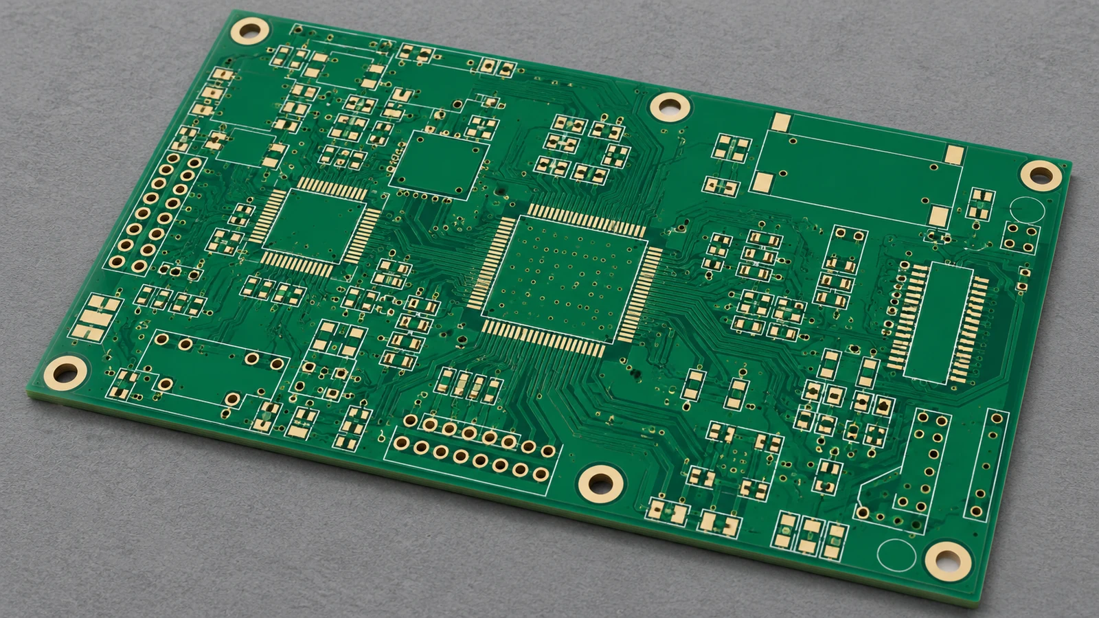
PCB assembly solder mask design determines which copper surfaces remain exposed for soldering and where insulating mask separates nearby features. Approve openings against the component land pattern, fabrication tolerances, and assembly inspection plan—not a universal sliver-width rule. For example, a 0.40 mm pitch with 0.25 mm pads and 0.075 mm mask expansion per side leaves zero nominal web between pads. That geometry needs an approved alternative opening strategy, not an assumption that a fine mask bridge will survive production. [1]
- Connect Solder-Mask Geometry to the Intended Solder Joint
- Compare Mask-Defined and Copper-Defined Pad Boundaries
- Review Openings, Registration and Fine Mask Slivers
- Calculate the nominal web before discussing capability
- Separate registration from opening-size variation
- Check Closely Spaced Pads for Bridging and Inspection Risks
- Before assembly: compare the delivered boundary
- After printing: examine the deposits separately
- After reflow: match the method to the accessible joint
- Resolve Mask Data Against the Package Land Pattern
- Compare recommendations without combining their assumptions
- Control the released data and applicable specifications
- Document Fabrication and Assembly Approval of Exceptions
- Apply the Review to Five Assembly Situations
- A fine-pitch QFN with nearly touching openings
- A DSBGA whose mask clips one side of a pad
- A QFN corner beside a via or exposed trace
- A repeated footprint after a board-source change
- A bridge reported after assembly
- Next Step: Submit a Joint-Geometry Review Package
Connect Solder-Mask Geometry to the Intended Solder Joint
Solder-mask geometry must preserve the solderable boundary intended for each connection. The review starts with the copper land, the opening around or within it, and the component termination—not with mask color or a default clearance setting. Permanent mask helps limit unwanted solder attachment, but its presence does not by itself establish an acceptable joint. [6]
Keep copper, solder mask, and solder paste as separate design objects. Copper defines the conductive land. The mask opening determines which part of that land and its surroundings is exposed. The stencil aperture determines where paste is deposited; stencil thickness and printing behavior also affect the deposited volume. A mask opening is therefore not a ready-made stencil aperture. 9
State the intended outcome before adjusting a footprint: preserve an exposed copper perimeter, maintain intentional overlap on a mask-defined pad, separate adjacent solderable areas, or keep a nearby trace covered. Then review the same location through the manufacturing sequence:
Package land pattern → copper/mask/paste overlay → fabrication geometry approval → incoming bare-board check → paste-print check → post-reflow joint inspection → exception closure.
Each step answers a different question. Does the drawing describe the intended joint? Can the fabricator reproduce the boundary? Did the delivered board preserve it? Did printing place separate deposits where required? Did reflow produce the required connections? Do not replace these questions with a single “DFM passed” label.
When a bridge appears, treat the mask as one candidate contributor. Compare the actual board, paste deposit, component position, and process record before identifying a root cause. A missing web is evidence of a geometry difference; it is not proof that mask geometry alone caused the bridge.
Compare Mask-Defined and Copper-Defined Pad Boundaries
Mask-defined and copper-defined pads differ in which feature sets the solderable boundary. A solder-mask-defined pad, abbreviated SMD here, has mask overlapping the copper perimeter. A non-solder-mask-defined pad, or NSMD, has an opening larger than the copper land, leaving its perimeter exposed. “SMD” in this comparison means solder-mask-defined, not surface-mount device. [3]
NSMD exposes the copper edge and top for solder wetting; SMD intentionally confines the solderable area inside a larger copper feature. Geometry belongs to the specific package and connection, not a board-wide rule. The referenced DSBGA recommendation favors NSMD for its stated packages; it does not authorize removing intentional overlap from another footprint.
Use the following matrix to connect each feature to a decision and its supporting evidence.
| Mask Feature | Joint-Formation Effect | Geometry to Review | Inspection Concern | Approval Evidence |
|---|---|---|---|---|
| Mask-defined pad | Mask opening bounds the exposed solderable area within a larger copper land. | Opening size, copper overlap, and worst-case registration at every edge. | Unintended copper-edge exposure or a displaced exposed area. | Package recommendation, overlap tolerance analysis, and approved fabrication detail. |
| Non-mask-defined pad | Exposed copper perimeter participates in wetting. | Clearance around the full land and mask coverage over adjoining traces. | Mask encroachment that changes the intended joint boundary. | Copper/mask overlay and agreed minimum finished clearance. |
| Mask expansion | More clearance protects pad exposure but consumes space between openings. | Per-side expansion, total opening dimension, and nearby copper. | Unintended exposure of another pad, trace, or via. | Dimensioned opening and tolerance check against neighboring features. |
| Narrow mask web | Retained mask separates neighboring openings. | Narrowest neck, length, corner shape, and finished-process limits. | Missing, damaged, or lifted mask; differences between artwork and boards. | Fabricator acceptance of the local geometry and inspection criteria. |
| Shared opening | Multiple isolated copper lands remain inside one mask-free region. | Entire opening boundary, copper separation, and separate paste deposits. | Bridges and exposed routing within the grouped opening. | Package rationale, assembly review, and defined joint-inspection coverage. |
| Mask near vias | Coverage determines whether neighboring via copper or an opening is exposed. | Pad-to-via relationship, mask boundary, and agreed via condition. | Unintended wettable paths or a via condition unlike the approved drawing. | Linked mask and via-treatment approvals with incoming-board evidence. |
The matrix is a review framework, not an acceptance standard. Use it to identify what needs measurement and who must agree. Keep via filling, plugging, and cap construction in the separate via-in-pad review; the mask review needs the approved resulting surface condition, not a second via-process specification.
Review Openings, Registration and Fine Mask Slivers
Openings, registration, and sliver survival require separate checks because they describe different geometries. Expansion is a nominal design offset; registration is the displacement of mask relative to copper; a web is the remaining mask between openings. A sliver is a locally narrow remnant, often at a neck or corner. Passing one check does not demonstrate the others. 2
Calculate the nominal web before discussing capability
For equal-width rectangular pads in a straight row, use this first-pass relationship along the pitch direction:
Nominal web = pad pitch − copper-pad width − left-facing expansion − right-facing expansion.
For equal expansion on both facing edges, the last two terms become twice the per-side expansion. The calculation concerns the artwork geometry; it does not predict the finished web after processing.
In the opening example, 0.40 − 0.25 − 2 × 0.075 = 0.000 mm. Reducing expansion to 0.060 mm per side leaves 0.030 mm nominally. This illustrates the fine-pitch LFCSP conflict: recommended mask clearance can consume the available pad spacing. Neither calculation proves that fabrication can retain a reliable mask web.
Use the actual shortest distance for rounded, staggered, or unequal pads. A row calculation can miss a smaller diagonal gap at a corner. Check the mask-free region around nearby tracks as well as the gap between component pads.
Separate registration from opening-size variation
For an NSMD edge, a conservative one-direction clearance check is:
Minimum clearance = nominal expansion − registration toward the pad − inward opening-edge variation − outward copper-edge variation.
Use bounded tolerances agreed with the fabricator. A quoted full opening-width tolerance is not automatically a per-edge tolerance. Likewise, an X/Y registration allowance is not automatically a radial allowance. Ask what the measurement references and what the supplier’s quoted capability already includes before combining terms; do not count a bundled allowance twice. Compare the calculated result with the agreed minimum finished clearance, not merely with zero.
A uniform translation of the mask changes its registration to copper but does not change the distance between two openings that move together. Opening-size variation, local distortion, and processing can change the web itself. Do not subtract the same global registration allowance from nominal web width as though it independently moved both facing edges inward.
For SMD, perform the complementary check: preserve the required mask overlap despite displacement and edge variation. Check the exposed opening’s location relative to the component termination too. A copper land can remain partly covered while the intended contact region moves out of position.
A narrow drawn web must also survive imaging and processing. The referenced supplier publishes different mask rules for different process conditions and states that undersized mask segments can be removed during data preparation. Its figures describe its own service; they are not universal minima or JASPER capabilities. Request the proposed production artwork whenever removal or resizing affects a critical footprint. [2]
Check Closely Spaced Pads for Bridging and Inspection Risks
Closely spaced pads should be reviewed as a combined geometry, printing, and inspection problem. A retained mask web cannot compensate for every paste or placement problem, and a shared opening does not automatically create a solder bridge. Establish which physical condition must be demonstrated before deciding whether to preserve, remove, or redesign a web.
Before assembly: compare the delivered boundary
For incoming bare boards, inspect the actual mask relative to copper at critical locations. Measure remaining clearance or overlap, identify unexpected exposed conductors, and compare narrow segments with the approved artwork. IPC-A-600 addresses bare-board mask coverage, registration, and adhesion-related conditions; apply the criteria invoked by the purchase specification rather than inventing a visual rule from a CAD screenshot. [7]
Record coordinates, board side, reference designator, and a scale with the image. A close-up without these identifiers cannot reliably distinguish a local geometry problem from a different footprint revision. Compare several relevant locations when deciding whether a discrepancy is isolated or repeats across the board.
After printing: examine the deposits separately
For a grouped opening, check whether the stencil still produces the intended separate deposits. Compare paste location, spread, and quantity against the assembly process requirements. The referenced supplier explicitly distinguishes customer paste data from assembly-process-adjusted stencil data; its workflow illustrates why a released mask layer should not be treated as the final paste program. [10]
Preserve the pre-reflow evidence when investigating bridges. A post-reflow image alone cannot show whether paste deposits were already connected or whether the board arrived with an unexpected opening. Record the observation first, then test the suspected mechanism.
After reflow: match the method to the accessible joint
Use optical inspection for accessible features and a suitable X-ray method for hidden-joint questions. QFN/SON inspection guidance includes optical and X-ray examination because much of the connection lies beneath the body. The package termination style also matters: a pull-back terminal and a wettable-flank terminal do not present the same visible fillet. [5]
Define the defect and verify that the inspection setup can distinguish it. Absence of bridging does not prove wetting at a concealed interface. Resolve ambiguous images with agreed additional verification before disposition. Micro-sectioning can support process optimization; that role does not make it routine production inspection.
Keep unresolved hidden-joint questions open rather than treating a clear top-side image as confirmation. Review acceptance against the actual termination geometry and applicable requirements, not an expectation that every package must show identical side fillets.
Resolve Mask Data Against the Package Land Pattern
Mask data should be resolved against the exact component package recommendation and the intended fabrication process. Check the ordering code, package drawing, footprint revision, copper layer, mask layer, and paste layer together. Where a family-level application note and a device-specific drawing differ, escalate the conflict to the design authority and component supplier instead of silently choosing the easier geometry.
Compare recommendations without combining their assumptions
The following sources demonstrate why pitch alone cannot select an opening strategy. Opening enlargement means the total dimensional increase unless a per-side clearance is explicitly stated.
| Primary source | Package context | Published mask guidance | Review implication |
|---|---|---|---|
| AN-772 | LFCSP perimeter lands | Describes individual openings at 0.50 mm pitch and above; uses a trench example at 0.40 mm pitch with 0.25 mm pads. | Match the land dimensions before copying the individual-versus-trench decision. |
| AN1902, Rev. 9 | QFN/SON perimeter lands | Gives 0.12–0.15 mm total opening enlargement, equivalent to 0.060–0.075 mm per side. | Evaluate clearance and remaining web together, with fabricator capability. |
| SLUA271C | QFN/SON perimeter lands | Describes individual openings for 0.65 mm pitch and above and grouped row openings at 0.50 mm pitch. | Do not replace this recommendation with another vendor’s pitch threshold. |
| SNVA009AI | DSBGA/WCSP lands | Favors NSMD and directs pad-geometry selection to device information. | Use the exact device land pattern rather than applying QFN row rules to a ball array. |
These recommendations serve different package and process contexts. Their differences should trigger a documented choice, not an averaged pitch threshold. A proposed departure needs the actual geometry, the reason for changing it, and a validation plan accepted by the responsible parties.
Control the released data and applicable specifications
Confirm whether each plotted mask shape represents an opening. Check positive expansion, zero expansion, and negative expansion as distinct CAD settings: they enlarge, match, or shrink the nominal opening relative to copper. None is an independent fabrication guarantee. Inspect exported geometry, including local overrides, instead of relying only on a global setting. [9]
Use IPC-SM-840 for the relevant solder-mask qualification and performance requirements, IPC-A-600 for bare-board acceptability, and IPC-A-610 for assembled-product visual acceptance, as invoked by contract. Specify the applicable revision and product requirements in the release package. These documents serve different purposes; an assembly acceptance criterion does not authorize modifying the customer’s design. 6 [8]
Release copper, mask, paste, fabrication notes, and the approved exception record as a consistent revision. Require a before-and-after overlay for any proposed CAM change that alters pad exposure, merges openings, or reveals nearby copper. Close the discrepancy before an order proceeds on an undocumented interpretation.
Document Fabrication and Assembly Approval of Exceptions
A solder-mask exception requires design authorization and the agreement of the parties responsible for making and inspecting it. The fabricator confirms the manufacturable mask condition; the assembler evaluates printing and joint formation; the design owner accepts the changed geometry. Quality defines how conformity will be demonstrated. Do not use a supplier’s DFM comment as a substitute for that decision.
| Responsible role | Decision to record | Required evidence | Release hold condition |
|---|---|---|---|
| OEM design authority | Accept or reject the changed land boundary or opening strategy. | Package rationale and marked-up before/after geometry. | Design intent or package compatibility remains unresolved. |
| PCB fabricator | Confirm the proposed finished mask and registration limits. | Process-specific tolerances and production-artwork disposition. | Critical overlap, clearance, or web retention cannot be committed. |
| Assembly engineer | Accept the printing and joint-formation approach. | Stencil review and defined first-build verification. | Deposits or solderable boundaries are not supported by the process plan. |
| Quality engineer | Define inspection, sampling, and disposition requirements. | Acceptance references, measurement method, and traceable records. | Critical features lack an agreed verification route. |
An exception record should identify the board revision, affected locations, original condition, proposed condition, reason, tolerance assumptions, approvers, inspection requirements, and applicability to future orders. Distinguish a one-lot concession from a permanent design revision. Set a disposition for boards already fabricated so that obsolete and revised configurations are not mixed.
Approval has two stages. Before manufacture, authorize the geometry and verification plan. After the build, close any required validation against the collected results. A promise to inspect later is not evidence that the resulting boards or joints already conform.
Apply the Review to Five Assembly Situations
Solder-mask review becomes actionable when each situation has a specific question, evidence request, and release condition. Use these five application situations to identify the decision needed before releasing or accepting the affected boards.
A fine-pitch QFN with nearly touching openings
Calculate the remaining web from the actual lands and opening offsets. When the drawing leaves no space for a web, compare the package’s grouped-opening option with a permitted land-pattern change. Release only after the fabricator and assembler agree on the final boundary and verification plan; shrinking clearance merely to clear a warning is not enough.
A DSBGA whose mask clips one side of a pad
Compare measured mask displacement with approved NSMD clearance and copper dimensions. Confirm that delivered geometry preserves the specified pad boundary. Separate fabrication deviation from inadequate nominal design before adjusting placement. Begin with the selected DSBGA package’s land requirements, not a generic mask rule.
A QFN corner beside a via or exposed trace
Overlay the mask opening, adjacent copper and package underside detail. Exposed metal near the pin-1 region can contact nearby features; check whether the proposed edit uncovers copper there. Keep the agreed via surface condition tied to the decision without redesigning the entire via structure.
A repeated footprint after a board-source change
Compare the new fabricator’s finished-feature tolerances and CAM disposition with the previous release. Require explicit confirmation of critical webs, not just a quotation using the same Gerber files. Retain source-specific inspection evidence. Identical input artwork does not establish identical commitments from two manufacturing processes.
A bridge reported after assembly
Collect the incoming-board image, paste-print evidence, placement information, and post-reflow inspection for the same location. List the observations before selecting a cause. If mask removal is implicated, compare the approved artwork with the board; if it is unchanged, investigate the remaining process candidates rather than redesigning the mask without evidence.
Frequently Asked Questions
PCB assembly solder mask design questions should be answered against the package, finished geometry, and release responsibilities. These answers summarize the review decisions above.
What is the difference between mask-defined and non-mask-defined pads?
Mask-defined pads have solder mask overlapping the copper, so the opening defines the solderable boundary. Non-mask-defined pads have a larger opening that exposes the copper perimeter. Choose the construction specified for the package and verify that manufacturing tolerances preserve its intended overlap or clearance.
Can a narrow solder-mask sliver always be manufactured reliably?
No. A sliver that exists in CAD may be removed during data preparation or may not meet the fabricator’s finished-feature requirements. Its narrowest width, shape, and process conditions matter. Obtain explicit fabrication agreement and an inspection criterion rather than applying one minimum width to every board.
How can mask misregistration affect assembly?
Mask misregistration can cover copper intended for soldering or expose copper intended to remain protected. On a mask-defined pad, it can move the exposed area relative to the termination. Review the finished geometry and tolerance budget; a placement correction cannot restore an incorrectly manufactured mask boundary.
Should adjacent fine-pitch pads share a mask opening?
Only when the package recommendation and joint process review support that arrangement. A shared opening can avoid an unmanufacturable web, but separate copper lands and appropriate paste deposits remain necessary. Check nearby routing and inspection coverage, and obtain design, fabrication, and assembly agreement before changing individual openings.
Who should approve a mask change suggested during assembly DFM?
The OEM design authority should authorize a change to the released mask geometry, with fabrication and assembly agreement and quality input on verification. Record the affected locations, before-and-after condition, acceptance evidence, and revision or concession scope. An assembly DFM suggestion alone is not approval to alter production data.
Is solder-mask expansion the same as a stencil aperture adjustment?
No. Solder-mask expansion changes the exposed board area; a stencil aperture adjustment changes paste deposition. The two must be reviewed together but are not interchangeable. Preserve separate mask and paste data, and evaluate any opening change for its effect on the approved printing approach and joint boundary.
Can optical inspection confirm every joint affected by a mask exception?
No. Optical inspection can assess accessible features, but hidden connections require an appropriate verification method. Use package-specific inspection requirements and a suitable X-ray approach where needed. Identify the defect being assessed and retain supporting evidence; a clear top-side image does not establish acceptance of every concealed joint.
What should an OEM send for a solder-mask design review?
Send the board revision, copper and solder-mask data, paste data, exact component package references, fabrication notes, and marked critical locations. Include any proposed CAM edits and available defect images. Request a written decision covering finished geometry, manufacturing tolerances, inspection requirements, and responsibility for approving each exception.
Next Step: Submit a Joint-Geometry Review Package
A solder-mask review package should make every critical opening traceable to a component, drawing revision, and acceptance decision. Mark the locations where pad exposure, web retention, grouped openings, or adjacent vias need agreement. Include the actual exported copper, mask, and paste layers rather than screenshots alone.
For a project with JASPER, submit those files with your PCB assembly services inquiry and identify the decisions needed before release. Request a consolidated fabrication-and-assembly response, resolve design exceptions in writing, and carry the approved geometry into the first-build inspection plan.
Ready to Start Your Project?
Tell us about your membrane switch, keypad, or graphic overlay requirements. Our engineering team will review your specifications and provide a detailed quote.