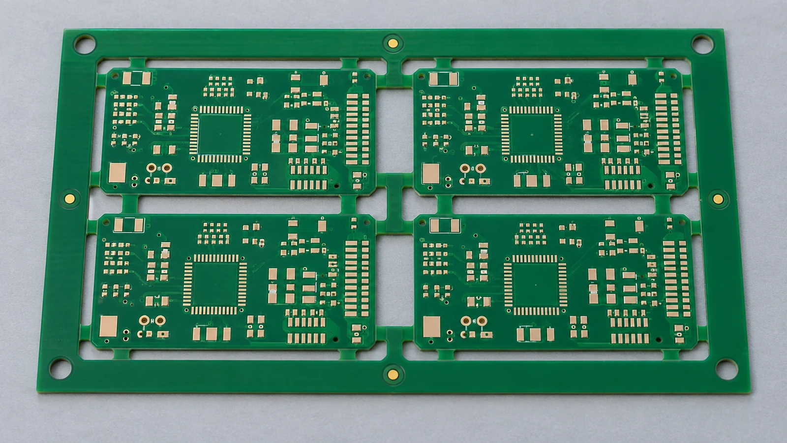
PCB assembly fiducials are optical reference targets formed in a board’s copper pattern so assembly equipment can relate physical positions to design coordinates. Board-level references align an individual PCB; panel references locate an array; local references support alignment around a selected component. Review these scopes separately, then confirm target visibility and the correction method used by the actual placement process. A usable fiducial plan requires more than circles in a layout: it needs recognizable finished targets, consistent coordinates and evidence that the intended component locations are reached.
- Global, Local and Panel Fiducials Serve Different Alignment Tasks
- Understand what the reference points can establish
- Show Fiducial Placement in Board and Panel Views
- Board view: separate whole-board and package references
- Panel view: make the board instances explicit
- Review Shape, Finish and Optical Contrast
- Check Solder-Mask Clearance and Nearby Visual Features
- Confirm Which Components Need Local Alignment Review
- Use Process-Specific Dimensions and Release Specifications
- Validate the Fiducial Plan with the Placement Process
- Five Application Scenarios for Fiducial Review
- Compact single-board controller
- Repeated boards in a manufacturing panel
- Fine-pitch processor or high-density package region
- Double-sided assembly
- Transfer to another assembly provider
- Next Step: Submit a Defined Alignment Plan
Global, Local and Panel Fiducials Serve Different Alignment Tasks
Global, local and panel fiducials differ by the area they reference, not simply by their diameter. In this article, board-level means global alignment of one PCB, panel means alignment of the complete array, and local means alignment around a component or compact component region. Some assembly documentation calls each board’s references “local” relative to its panel. Identify the reference scope on the drawing instead of relying on the name alone.
Understand what the reference points can establish
A circular target supplies a center position, not an orientation by itself. Separated targets provide a baseline for determining rotation. Three non-collinear reference positions can support a more detailed planar transformation when the software implements it. This is a geometry distinction, not a promise that adding another mark improves every machine.
The reference placement implementation uses two points for estimation with average scaling, three points for separate axis scaling and non-squareness, and additional points for averaging. Confirm the actual machine’s supported transformation. Correcting coordinates within a plane does not flatten a bowed PCB or locate every locally distorted pad.
Use the following matrix to assign an alignment task and a review owner before approving the layout. Agree the recognition and correction methods with the assembler, then record the evidence needed to close each check.
| Alignment Feature | Reference Scope | Location Check | Optical Requirement | Process Confirmation |
|---|---|---|---|---|
| Panel fiducial | Complete manufacturing array | Locate on material retained and visible during the relevant operation; identify panel orientation | Distinct target and surrounding image area, unobstructed by handling hardware | Confirm panel acquisition and the mapping to individual board positions |
| Board-level fiducial | One PCB within or outside an array | Spread references across that PCB; identify each board instance | Repeatable target appearance on the processed side | Confirm whether the program reacquires each board or uses panel-derived coordinates |
| Local fiducial | Selected package or component region | Relate the marks to the package’s land pattern and recognition sequence | Readable when the local alignment operation occurs | Confirm which placements receive the local correction |
| Solder-mask clearance | Target boundary and immediate background | Check the released mask opening against copper and fabrication tolerances | Target edge remains exposed and distinguishable | Approve the manufactured appearance, not only the CAD view |
| Nearby copper and markings | Camera search neighborhood | Review pads, vias, legend, labels and panel features around the target | No competing feature produces a plausible wrong match | Verify target identity within the programmed search region |
Show Fiducial Placement in Board and Panel Views
Review both board and panel fiducial views. The board view identifies references associated with its circuitry; the panel view relates them to array orientation and handling. The i.MX layout example distinguishes board and component references. Keep global and local reference roles explicit in the drawings.
Board view: separate whole-board and package references
BOARD VIEW — viewed from the side being assembled
+------------------------------------------------------+
| o B1                                          o B2   |
|                                                      |
|               o L1                                   |
|                    +----------------+                |
|                    | U1 land-pattern|                |
|                    |     region     |                |
|                    +----------------+                |
|                                       o L2           |
|                                                      |
| o B3                                                 |
+------------------------------------------------------+
B1/B2/B3: board-level references
L1/L2: a possible local pair associated with U1
Figure 1. A conceptual three-point board arrangement with a separate local pair. The letters are explanatory labels, not instructions to print legend beside the targets. The circles represent optical copper features, not drilled holes. Placement is schematic and not to scale; the illustrated count is not a universal requirement.
Panel view: make the board instances explicit
PANEL VIEW — viewed from the side being assembled
+------------------------------------------------------+
| o P1                                          o P2   |
|       +------------------+  +------------------+     |
|       | o A1       o A2  |  | o B1       o B2  |     |
|       |                  |  |                  |     |
|       |     BOARD A      |  |     BOARD B      |     |
|       |                  |  |                  |     |
|       | o A3             |  | o B3             |     |
|       +------------------+  +------------------+     |
| o P3                                                 |
+------------------------------------------------------+
P1/P2/P3: panel references on retained border material
A1/A2/A3 and B1/B2/B3: separate board-reference sets
Figure 2. Panel acquisition and individual-board acquisition are separate decisions. Drawing both sets makes the intended reference hierarchy reviewable; it does not instruct a machine to use them automatically.
Annotate the actual release drawing with fiducial identifiers, center coordinates, units, side and coordinate origin. State whether a bottom-side view is seen from below or mirrored from above. Identify rotated board instances explicitly rather than expecting the programmer to infer their orientation from repeated artwork.
Overlay the assembler’s clamping and camera-access boundaries on the proposed targets. An exposed center is insufficient when the surrounding recognition area is obstructed. Keep this review focused on reference visibility; rail construction and separation methods belong in the broader panelization review.
Review Shape, Finish and Optical Contrast
Match fiducial shape, finish and contrast to the vision method. A solid circular target is a useful candidate because in-plane rotation does not change its outline. One reference placement system requires round targets; a flip-chip BGA layout example permits a circular target with a separate optional outer ring. These patterns are not interchangeable library symbols.
Use a dedicated copper feature, not a legend dot. The referenced layouts use etched copper targets with protective coating or plating and electrically unconnected fiducial pads. Preserve the target’s relationship to the component copper pattern instead of redefining it through printed markings.
For finish review, compare the manufactured target with the board drawing and the camera image. Ask whether the visible edge remains continuous, whether reflections obscure part of the outline, and whether repeated acquisitions identify the same center. Do not approve a target merely because it appears bright in a photograph.
Include the specified surface finish in that comparison. A plated target and a solder-levelled target should not be assumed to give the same image under unchanged illumination. The practical review is to test representative boards, rather than prescribe a finish solely from its color or demand the most reflective surface.
Keep applied solder paste off dedicated optical targets; this is separate from the board’s specified protective finish. The referenced supplier identifies paste exclusion as an important fiducial consideration. Review paste data as well as copper and mask data so a footprint-library setting does not create an unintended paste deposit.
Check Solder-Mask Clearance and Nearby Visual Features
Keep solder mask from encroaching on the fiducial. The opening must expose the intended target edge without creating a confusing recognition neighborhood. Check copper geometry, mask opening and nearby visual features separately; one clearance value cannot describe all three.
For concentric circular geometry, define the dimensions explicitly:
Dc = copper target diameter
Dm = solder-mask opening diameter
c  = nominal radial gap from copper edge to mask edge

c = (Dm - Dc) / 2
This relationship is geometry, not a recommended footprint. A drawing that gives an opening diameter is not specifying the same quantity as a radial gap. Fabrication variation and mask registration can reduce the actual clearance on one side; have the fabricator assess the drawing tolerances rather than treating nominal concentricity as guaranteed.
Separate the mask opening, optical keep-out and camera search radius. The keep-out controls the neighborhood around the target; the search radius limits where software can accept a match and is distinct from target diameter. Enlarging the mask opening cannot by itself correct a search region that admits the wrong circular feature.
Inspect exported copper, mask, paste and legend layers together, then view an actual target through the placement camera. Check whether a nearby pad, via, curved trace or repeated mark could be mistaken for the fiducial. Similar-looking neighbors can defeat otherwise suitable target geometry.
Do not solve a vision problem by deleting electrically necessary copper or changing a package land pattern without design approval. First establish which feature is being selected and why the search admits it. A misplaced search region, changed artwork and an obscured target need different corrective actions, even when the machine reports the same recognition failure.
Confirm Which Components Need Local Alignment Review
Review local fiducials when the selected board-level references may not meet package placement needs. The i.MX layout example recommends component fiducials for fine-pitch parts, but their usefulness also depends on board and equipment. Resolve the package-specific requirement; do not infer a universal pitch cutoff.
Start with the package land pattern, permissible placement offset, location on the board and evidence from the intended process. Ask the assembler to explain how the component’s board coordinates are established and which references support that calculation. A statement that a machine recognizes component leads does not answer the board-registration question: the referenced supplier describes board-target recognition and component optical centering as distinct operations.
For a proposed local pair, identify the package region it serves and when the targets are read. Avoid a plan that requires reacquiring a mark after the mounted component or another assembly feature has hidden it. When several components share a reference pair, have the programmer explicitly assign that common correction region.
Before requesting more local marks, distinguish registration error from incorrect package data, component centering or an origin mismatch. Adding references cannot repair the wrong land pattern or wrong placement coordinates. Preserve evidence of the observed offset and its location so the review addresses the demonstrated problem rather than the component’s name alone.
Use Process-Specific Dimensions and Release Specifications
PCB assembly fiducial dimensions should come from an accepted process specification or a project-approved footprint. Published recommendations differ in their target geometry and operating context. The examples below preserve those distinctions; they are not universal minimum sizes or JASPER capability limits.
| Published source and context | Copper target example | Surrounding geometry described | How to use the recommendation |
|---|---|---|---|
| The referenced supplier, “Finding fiducials,” its assembly-process discussion | 1.5 mm preferred example; 0.6 mm also discussed where space requires | A centered mask opening is part of the target construction | Discuss a selected footprint with the receiving assembler; the smaller example is not a general industry minimum |
| DLP9500UV, Rev. E | 0.05 inch, equivalent to 1.27 mm | 0.1 inch, equivalent to 2.54 mm, described as a cutout or antipad | Retain the specification’s terminology and define its layer implementation in the project drawing |
| SPRU811A | 1.6 mm circle | Optional annulus specified as 3.175 mm/3.71 mm; the guide also specifies 0.76 mm separation from other features | Evaluate the complete target pattern; do not interpret the annulus dimensions as a solder-mask opening |
| Round-target detector reference implementation | 1 mm circle | 2 mm diameter keep-out for mask and other copper | Treat this as a software-specific reference arrangement, not a general assembly standard |
The figures are individual published examples, not a catalog of mandatory size grades. Do not average them, convert them into a universal range, or combine one source’s copper diameter with another source’s surrounding geometry without reviewing the resulting target.
Approve a complete footprint definition: copper shape and dimensions, dimensional tolerances, mask opening, paste exclusion, finish and optical keep-out. Then confirm its compatibility with the selected assembly process. The acceptance criterion is correct, repeatable recognition and satisfactory placement under the agreed conditions—not the largest diameter that fits.
The governing release should identify the board and panel revisions, applicable package guidance and the assembler’s accepted vision requirements. Where a contract invokes an IPC document, identify the required edition and applicable provisions. A supplier article or component application note should not be converted into an unqualified claim about an IPC minimum.
Validate the Fiducial Plan with the Placement Process
Fiducial validation should demonstrate that the approved reference plan works on representative manufactured boards in the intended assembly sequence. Separate document agreement, image recognition and placement evidence in the release workflow. A drawing check alone does not qualify the placement process.
Agree reference scopes and board/panel revisions
  -> Review copper, mask, paste and visibility
  -> Confirm references selected in the placement program
  -> Acquire targets on representative production-condition boards
  -> Check resulting placement against the agreed requirements
  -> Record approval and the changes that require reassessment
| Review stage | Responsible function | Evidence to retain | Release decision |
|---|---|---|---|
| Layout agreement | PCB designer and assembly engineer | Annotated board/panel views with side, origin and fiducial identifiers | All intended reference scopes are explicit |
| Manufactured target review | Fabricator and assembly engineer | Finished-target images and disposition of drawing deviations | Copper, finish and mask condition support the selected recognition method |
| Program agreement | Placement programmer | Reference assignments, board-instance mapping and vision recipe identification | The program uses the approved targets for the intended placements |
| Placement confirmation | Assembly and quality engineers | Acquisition observations and placement inspection against project criteria | Correct recognition and acceptable placement are both demonstrated |
| Change control | Project owner with affected functions | Comparison of changed data or process conditions with the approved baseline | Reassessment is completed where the reference plan is affected |
Use the process condition that matters. In the referenced supplier’s described SMT sequence, placement follows paste printing. Include the applicable paste-printed and second-side states in the review rather than relying only on an untouched bare-board sample. Record the surface condition and handling arrangement with the observations.
Choose inspection locations that challenge the reference hierarchy. For an array, include relevant corner and interior board instances in the agreed trial; for a local correction, include its assigned package region. Agree the sample quantity and repeat-loading checks with the responsible engineers. Retain the program and vision-recipe revision so later comparisons use an identifiable baseline.
Investigate both a failure to recognize and a successful match to the wrong feature. Capture the image, intended identifier, selected location and affected board instance. Repeatedly selecting the wrong pad is repeatable behavior, but it is not valid alignment.
Agree acceptance criteria before the trial, including how placement will be checked and what requires a hold. Do not invent a universal vision-score threshold or retry allowance. Keep machine calibration and maintenance in their separate controlled procedures; this review establishes whether the design and released process are compatible.
Five Application Scenarios for Fiducial Review
Fiducial review changes with the board’s reference hierarchy and assembly sequence. These five application scenarios show which reference relationship, process condition or release decision to examine next.
Compact single-board controller
For a small controller, review whether board-level acquisition supports every fitted package. Keep references available where the handling arrangement allows them, and document any accepted alternative. Do not consume scarce routing space with local targets unless the component review establishes their purpose. Recheck the arrangement when a finer-pitch device is introduced.
Repeated boards in a manufacturing panel
For a repeated array, distinguish locating the panel from locating each circuit instance. Confirm board numbering, orientation and any board-specific reference acquisitions. Check targets near variable labels or altered artwork separately. One accepted panel image should not be used as evidence that every board instance maps to the correct coordinates.
Fine-pitch processor or high-density package region
For a fine-pitch processor, inspect the relationship between its land pattern and the references actually used. Decide whether a local pair is needed from placement requirements and process evidence. Keep optical acquisition separate from inspection of hidden solder joints: fiducial recognition is not a solder-joint acceptance test.
Double-sided assembly
For a double-sided PCB, prepare a reference plan for each processed face. Confirm the side convention and which marks remain visible after the first assembly operation. Check the actual support and surface conditions during second-side acquisition. Do not assume that an accepted first-side recipe automatically validates the opposite side.
Transfer to another assembly provider
For a manufacturing transfer, send the accepted target definitions and reference hierarchy, not just their nominal diameters. The new provider should establish its own program assignments and recognition evidence. A process-specific decision to use an existing pad or omit dedicated marks needs renewed review rather than automatic inheritance from the previous build.
Frequently Asked Questions
These answers use the board, panel and component reference scopes defined above. Final acceptance belongs to the selected design and assembly process.
What is the difference between global and local PCB fiducials?
Global fiducials reference a whole board, while local fiducials reference a selected component or small component region. Panel references apply to the complete array. Because some suppliers call individual-board references local relative to a panel, identify the physical scope and the placements affected in the assembly drawing and program.
Are panel fiducials enough for every board in a panel?
No, panel fiducials are not automatically sufficient for every circuit instance. The assembler must establish whether panel-derived coordinates meet the placement requirements or whether individual-board acquisition is needed. Confirm the reference hierarchy, board orientations and placement evidence across the relevant instances rather than treating successful panel recognition as complete validation.
Can a component pad be used as a fiducial?
Yes, an assembler may approve an existing pad as a process-specific reference when its vision system can identify it reliably. Check the pad’s appearance at the acquisition stage, including paste and possible obstruction. Keep the pad’s electrical and soldering functions unchanged, and document the accepted alternative instead of assuming interchangeability.
Why do finish and mask clearance affect fiducial recognition?
Finish and mask clearance affect the target boundary and background presented to the camera. Mask encroachment can obscure the intended edge, while surface condition can change its visible appearance. Review the finished target with the actual vision settings and process state; a clean CAD symbol does not demonstrate successful optical recognition.
When should an assembler request local fiducials near a package?
An assembler should request local fiducials when the package’s placement requirements justify a reference closer to its land pattern and the process can use that reference effectively. Evaluate measured offsets, board location and the existing correction method. Package pitch or a BGA designation alone does not establish a universal requirement.
What size should PCB assembly fiducials be?
Use the complete footprint accepted for the intended assembly process, not a universal minimum diameter. Copper size, mask opening, optical keep-out and target pattern must be considered together. Published supplier examples are useful discussion inputs, but they do not establish another assembler’s capability or replace recognition and placement evidence.
Do double-sided PCBs need fiducials on both sides?
Each side undergoing optical alignment needs an accepted reference strategy for that operation. Dedicated marks on both faces are one approach; any alternative requires process approval. Verify side conventions, visibility and the condition after earlier assembly steps. References on one face do not automatically serve a camera viewing the opposite face.
Do fiducials need solder-paste openings?
Dedicated PCB fiducials should not receive printed solder paste. Their optical target is the finished board feature, so check the paste layer independently from the solder-mask opening. Stencil alignment features are a separate tooling matter and should not be confused with an instruction to deposit paste on a PCB fiducial.
Next Step: Submit a Defined Alignment Plan
A defined alignment plan gives the assembler specific decisions to review. Prepare the board and panel drawings, copper/mask/paste data, placement file, surface-finish specification and a list of packages requiring local-alignment review. Identify the approved revision and provide relevant images or observations from previous builds.
For an OEM project with JASPER, include these inputs when discussing PCB assembly services. Ask the engineering review to close reference scope, visibility, program assignment and placement acceptance together. Approve the plan only when the targets shown in the release data are the targets the intended process can use.
Ready to Start Your Project?
Tell us about your membrane switch, keypad, or graphic overlay requirements. Our engineering team will review your specifications and provide a detailed quote.