
Circuit Substrates and Conductive Inks
Membrane switch circuit materials should be selected as a complete electrical and mechanical system, not as isolated layers. A printed PET circuit may suit a thin, flexible interface; copper FPC may suit tighter routing or repeated bending; and a rigid PCB may suit component integration or a fixed support structure. The correct construction depends on the load, layout, tail, connector, enclosure, and validation requirements.
Quick Selection Facts
The circuit layer carries signals between the key area, components, tail, connector, and host electronics. The first decision is therefore not “Which material is best?” but “What must this circuit do inside the finished assembly?”
| Engineering input | Why it changes the circuit decision | Information to provide |
|---|---|---|
| Electrical load | The load and switching architecture affect conductor, trace, contact, and interface choices. | Circuit diagram, operating conditions, and the loads connected to each path |
| Routing density | Closely packed keys, indicators, or components can make routing and crossover strategy more important. | Key matrix, artwork, keep-out zones, and available circuit area |
| Flexing and installation | A circuit that bends during installation has different needs from one that remains flat or is repeatedly moved. | Bend location, bend direction, installation sequence, and available radius |
| Components | LEDs, resistors, connectors, or other parts can influence substrate and attachment decisions. | Bill of materials, placement drawing, polarity, and assembly constraints |
| Tail and connector | Tail length, exit direction, contact pitch, stiffener, and mating hardware are part of the circuit construction. | Connector reference, mating board details, tail drawing, and insertion method |
| Enclosure space | A low-profile laminate, flexible tail, or supported board must fit the actual enclosure stack. | Section drawing, fastening points, clearances, and compression conditions |
| Validation | Inspection and test requirements should be defined before the circuit is released. | Acceptance criteria, electrical test needs, drawing revision, and documentation requirements |
Circuit Construction Options
The following options describe common decision paths. They do not confirm a universal JASPER manufacturing range or guarantee that every construction is available for every project. Final selection should follow a review of the drawing, approved material records, and prototype evidence.
| Construction or material | Typical engineering role | Reasons it may be considered | Important limitations to review |
|---|---|---|---|
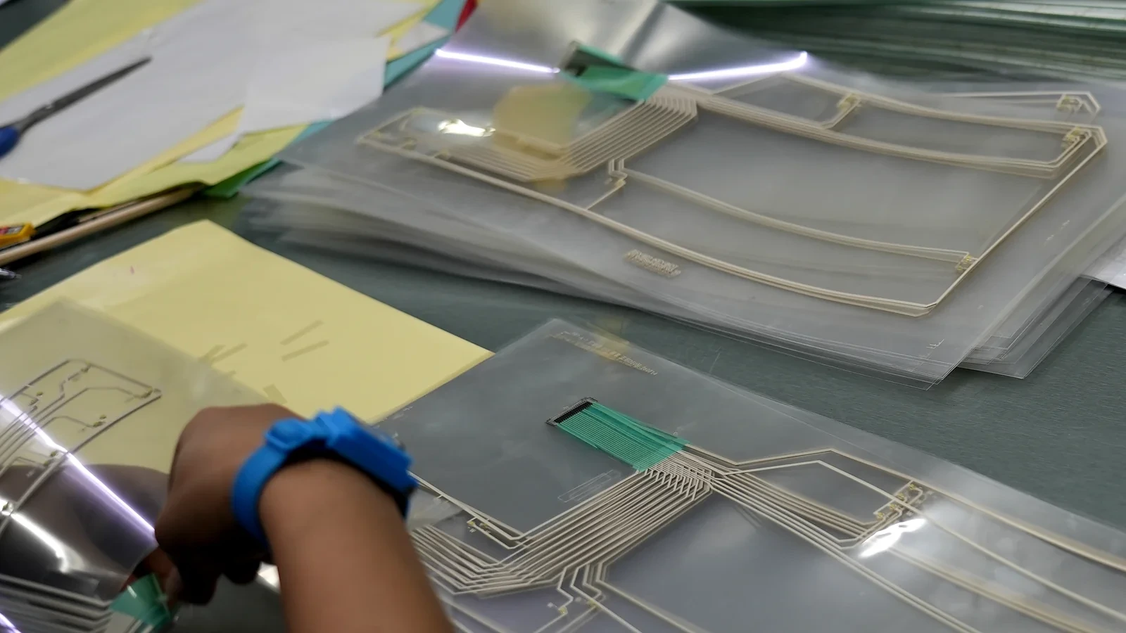
| Printed PET circuit with conductive ink | Thin flexible circuit layer for key matrices and interface tails | Can support a compact laminated construction and screen-printed routing | Trace geometry, bends, contact design, curing history, and electrical targets must be reviewed together |
| Carbon contact areas | Contact or interface surface within a printed circuit design | May be used where a defined contact surface is needed | Ink system, contact geometry, mating surface, contamination, and required electrical behavior remain project-specific |
| Copper FPC | Flexible copper circuit for denser routing, fine connector interfaces, or component integration | May offer a different routing and attachment path than a printed circuit | Stack thickness, bend handling, copper fatigue risk, finish, connector, and assembly method require verification |
| Rigid PCB | Supported circuit for fixed assemblies or more extensive component integration | May simplify mounting or provide a stable component platform | Board outline, enclosure clearance, fasteners, component height, sealing, and connection to the user interface must be coordinated |
| Dielectric or insulating layer | Separates conductive features and can support crossovers in an applicable printed construction | Helps control where electrical paths may cross or remain isolated | Registration, coverage, curing, adhesion, and inspection method must match the selected ink system |
| Tail stiffener | Supports the contact end of a flexible tail during insertion or mating | Can improve handling at the connector interface | Length, position, thickness, adhesive, exposed contacts, and connector geometry must be defined from the mating requirement |
For a commercial comparison of assembled options, see PCB and FPC membrane switch constructions.
Conductive and Insulating Materials
Conductive ink is one part of a printed circuit system. The substrate, conductor pattern, contact area, dielectric, crossover, tail, spacer, and mating surface all influence the result. Silver conductive ink may be considered for printed traces, carbon ink for selected contact features, and dielectric material for isolation or an applicable crossover strategy.
Exact ink systems, conductor properties, process conditions, finishes, and inspection limits must come from current supplier documentation and JASPER-approved project records. Copper FPC and rigid PCB constructions follow different material, component, connector, support, and enclosure paths, so their complete stacks must be reviewed rather than inferred from the substrate name.
How to Choose the Circuit Construction
Start with the electrical architecture, then test it against mechanical reality.
- Define the switching and load conditions. Identify each path, what it controls, and the conditions that affect conductor or contact selection.
- Map the routing area. Place keys, windows, indicators, components, connector exits, mounting features, and keep-out zones.
- Describe every bend. Separate installation bends from repeated movement and show how the assembler will route the tail.
- Lock the connector interface. Review contact pitch, exposed contacts, stiffener, insertion direction, and mating geometry together. See the membrane switch connector guide.
- Account for components. Confirm placement, attachment, polarity, clearance, and assembly sequence against the selected circuit.
- Plan validation before release. Define visual, electrical, dimensional, and documentation checks; use prototypes to resolve uncertain interfaces.
Current, resistance, routing density, and component needs cannot be reduced to a universal threshold on this page. The drawing and electrical requirements must drive the choice.
Manufacturing and Assembly Implications
For a printed circuit, artwork registration controls how traces, contacts, dielectric features, spacer openings, keys, and the tail align. Printing, curing, crossover, and inspection details must match the approved material system. During lamination, the circuit must also align with contacts, adhesive-free areas, windows, vents, and the overlay without pinching the tail or contaminating exposed contacts.
FPC and PCB constructions add component attachment, finish, cover-layer, support, and cleaning decisions. State those processes only after approval. Use electrical and circuit inspection to plan project validation, while keeping acceptance requirements on the released drawing.
Failure Modes to Review Before Approval
| Observed problem | Possible stack-level cause | Evidence to inspect | Corrective direction |
|---|---|---|---|
| Intermittent open circuit | Trace damage, contamination, connector movement, or misregistration | Artwork, bend history, contact area, connector fit, and test record | Isolate the failure location before changing materials |
| Cracked trace near a bend | Bend position, motion, handling, or routing | Tail drawing, installed sample, bend direction, and trace orientation | Revise routing, support, installation, or substrate as evidence indicates |
| Contact inconsistency | Contamination, geometry, mating surface, or material pairing | Contact images, spacer opening, alignment, and circuit interface | Review the complete contact stack, not only the ink |
| Silver migration concern | Moisture, contamination, voltage condition, spacing, or protection may contribute | Environment, conductor spacing, dielectric coverage, and failure analysis | Confirm root cause before making a durability claim |
| Tail or connector damage | Stiffener, insertion, contact geometry, or unsupported bending | Connector drawing, marks, stiffener position, and work instruction | Align tail design with the mating and assembly process |
| Delamination or movement | Surface, adhesive, process history, stress, or enclosure mismatch | Cross-section, material records, and installed stack | Correct the interface identified by inspection |
| Circuit registration error | Revision mismatch or layer alignment issue | Released files, fiducials, images, and continuity map | Restore revision control and verify registration |
Alternatives and Design Boundaries
This page explains material roles but does not replace circuit design review. The article on PCB versus printed-circuit membrane switches retains comparison intent.
If a laminated circuit cannot accommodate routing, components, mounting, or connector needs, an FPC, PCB, harness, or revised enclosure may be more appropriate. Choose from system requirements, not material preference.
Related Products, Testing, and Applications
- Custom membrane switch circuit constructions for a complete laminated switch stack.
- PCB and FPC membrane switches for a commercial circuit-product decision.
- Electrical and circuit inspection for project validation planning.
- Circuit tails, stiffeners and connector selection before tail artwork is locked.
- Industrial control interfaces when enclosure and field use affect the stack.
- JASPER Materials Center for the complete material-family overview.
Engineering FAQ
What material is used for a membrane switch circuit?
A membrane switch circuit may use a printed polymer-film construction, copper flexible circuit, or rigid PCB. The choice depends on the circuit diagram, routing area, bends, connector, components, enclosure, and validation plan.
When should a printed PET circuit be considered?
A printed PET circuit may suit a thin laminated interface and flexible tail. Trace layout, contacts, bends, electrical targets, ink system, dielectric features, connector, and assembly handling still require review.
What are silver and carbon inks used for?
Silver ink may be considered for traces and carbon ink for defined contact features. No current, resistance, durability, or compatibility value should be assumed without supplier documentation, an approved drawing, and project evidence.
Is FPC automatically better than a printed circuit?
No. FPC changes routing, bending, connector, finish, component, and assembly decisions. Printed PET, FPC, and PCB each fit different requirements; none is automatically superior.
What should be included in a circuit material review?
Provide the circuit diagram, key matrix, mechanical drawing, tail and bends, connector, components, load, enclosure clearances, assembly sequence, test requirements, and required records. Include mating samples when drawings do not fully describe the installation.
Send Your Circuit Requirements
Send the circuit diagram, key layout, routing area, electrical load, tail and bend details, connector, components, enclosure section, assembly method, and test expectations. JASPER can review candidate printed PET, FPC, or PCB constructions and identify items requiring prototype or material-record confirmation.
Review the Complete Stack Before Tooling
Share the drawing, enclosure, operating conditions, assembly process, approval evidence, quantity, and timing. Unknown values can remain open items; they should not become assumed guarantees.