Teclados de caucho conductivo
Un teclado de caucho conductivo usa una tecla de silicona moldeada y un elemento conductivo bajo la tecla para cerrar un circuito en PCB, FPC, circuito PET o membrane switch. El contacto mas comun es una pastilla de carbono porque es durable, rentable y compatible con pads de contacto impresos o metalizados. JASPER disena juntos la geometria del keypad, metodo conductivo, layout de contacto, objetivo de resistencia y stack de ensamblaje para que el teclado tenga buen tacto y conmute de forma confiable en produccion.
La conmutacion confiable empieza bajo la tecla
La mayoria de fallas en keypads de caucho no empiezan en la parte visible de la tecla. Empiezan debajo: una pastilla de carbono que no aterriza bien sobre el pad PCB, una superficie conductiva con resistencia inestable, un area de contacto contaminada, una forma de dome que llega al fondo antes de cerrar el circuito, o un layout de pads que se desgasta de forma desigual.
That is why we treat conductive rubber keypad design as an electrical and mechanical stack, not as a rubber molding job alone.
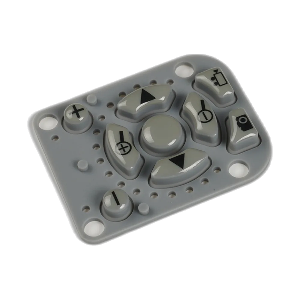
Un teclado de caucho conductivo tipico incluye:
- Una manta de teclas de silicona moldeada con geometria web ajustada
- Una pastilla de carbono, area de tinta conductiva, actuador metal dome o contacto metalico bajo cada tecla
- Un patron de contacto en PCB, FPC, circuito PET o membrane switch
- Spacer, adhesive, housing, or retaining features that control alignment
- Leyendas, recubrimientos, retroiluminacion y prueba electrica final opcionales
When the user presses the key, the molded dome collapses, the conductive contact touches the circuit pads, the circuit closes, and the rubber web returns the key to its starting position. The design goal is simple: the key should close every time, feel consistent from key to key, and keep working after real field use.
Conductive Contact Options
| Conductive method | Best fit | Notes |
|---|---|---|
| Carbon pill / graphite pill | Standard OEM silicone keypads | Common balance of cost, life, and PCB compatibility. Good for many industrial, medical, and consumer controls. |
| Conductive ink | Thin or area-specific conductive features | Useful when the conductive region must follow a custom shape, but it needs process control and wear evaluation. |
| Metal dome under silicone actuator | Crisp tactile snap with rubber key surface | Silicone key acts as the actuator while a stainless dome provides tactile feedback and switching. |
| Metal, nickel, or gold-plated pill | Lower-resistance or special contact requirements | Used when the electrical requirement is more demanding than standard carbon contact. |
| Non-conductive actuator | Key presses a separate switch | Best when the circuit already uses mechanical switches or domes on the board. |
For most projects, we start with carbon pills unless the circuit requirement, tactile feel, or life test target points elsewhere.
Carbon Pill Design Details That Matter
A carbon pill sounds like a small detail, but it decides whether the keypad works reliably.
Pill size and position
The pill must land on the PCB or circuit contact area with enough overlap even after molding tolerance, assembly tolerance, and normal key movement. If the pill is too small or too close to an edge, intermittent contact becomes likely.
Contact pad geometry
PCB pads often use interdigitated patterns, split pads, or plated contact areas. The pad design must match the pill diameter, expected pressure, contact resistance target, and contamination risk.
Actuation force and overtravel
The key should close the circuit before the user bottoms out harshly on the board. Good overtravel protects the contact and makes the key feel less abrupt.
Resistance target
Many carbon pill keypads do not need ultra-low resistance, but they do need stable resistance across keys and over life. We confirm the electrical target before choosing pill type, pad finish, and test method.
Clean assembly
Dust, silicone oil, release-agent residue, and handling contamination can all affect contact behavior. Conductive keypad assembly should include clean handling and inspection, especially for medical, automotive, or high-volume consumer electronics.
Conductive Rubber Keypad Stack Options
Conductive rubber keypads can close onto several circuit types.
| Circuit carrier | When to use it | Design concern |
|---|---|---|
| Rigid PCB | Durable control modules, LED integration, electronics on the same board | Pad finish, LED clearance, screw bosses, and housing stack-up |
| FPC | Compact handhelds, curved routing, connector flexibility | Tail bend radius, stiffener position, and contact alignment |
| PET printed circuit | Cost-sensitive or membrane-style assemblies | Silver ink thickness, spacer design, and environmental sealing |
| Membrane switch layer | Hybrid rubber + membrane HMI | Dome clearance, adhesive stack, and overlay/keypad interface |
| Separate mechanical switch | Tactile or high-force switch designs | Actuator height, switch tolerance, and housing datum control |
JASPER can provide the rubber keypad only, but most conductive keypad problems are easier to prevent when the keypad and circuit carrier are reviewed together.
Common Failure Modes We Design Against
| Failure mode | Typical cause | Prevention |
|---|---|---|
| Intermittent key response | Pill misses pad or contact pressure is too low | Increase pad overlap, adjust pill size, tune web geometry, verify stack height |
| High or unstable resistance | Contamination, wrong pill type, poor pad finish | Define resistance target, clean process, choose suitable contact material |
| Uneven key feel | Web thickness variation or inconsistent key geometry | Review DFM, mold flow, tool tolerance, and force-displacement samples |
| Premature contact wear | Hard bottoming, abrasive pad surface, inadequate overtravel | Add overtravel, adjust contact pressure, review PCB pad finish |
| Assembly misalignment | No positive datum between keypad, PCB, and housing | Add locating pins, bosses, ribs, or carrier features |
The best time to solve these issues is before the mold is cut.
Aplicaciones
Conductive rubber keypads are used wherever a molded key surface needs to close an electrical circuit reliably:
- Medical device front panels and handheld controllers
- Industrial machine controls, test equipment, and field instruments
- Automotive remote controls, seat controls, console buttons, and service tools
- Security panels, access control devices, and alarm interfaces
- Consumer electronics, appliance controls, and remote controls
If the same keypad also needs illuminated icons, see Backlit Teclados de silicona. If it needs to ship as a complete module with PCB and housing, see Silicone Keypad Assemblies.
RFQ Checklist
For a conductive rubber keypad quote, send:
- Keypad drawing or product layout
- PCB/FPC/PET contact layout if available
- Preferred conductive method, or ask us to recommend one
- Target actuation force, travel, and tactile feel
- Contact resistance requirement, if specified
- Key life requirement or application duty cycle
- Environmental exposure: water, oil, cleaning chemicals, dust, UV, temperature
- Required testing and documentation
- Annual volume and prototype schedule
Preguntas frecuentes
What is a conductive rubber keypad?
A conductive rubber keypad is a silicone rubber keypad with a conductive element under each key. When the key is pressed, the conductive element touches a circuit pattern on a PCB, FPC, PET circuit, or membrane switch and closes the circuit.
Are carbon pills the standard contact method?
Yes, carbon pills are the standard choice for many silicone rubber keypads because they are durable, economical, and compatible with common PCB contact patterns. Conductive ink, metal domes, metal pills, or non-conductive actuators may be better for special electrical or tactile requirements.
What causes intermittent contact in rubber keypads?
Common causes include poor carbon pill alignment, insufficient contact pressure, contaminated contact surfaces, inadequate pad overlap, incorrect stack height, or a keypad web geometry that does not allow clean overtravel after the circuit closes.
Can JASPER design the PCB contact pattern too?
We can review or help define the contact pattern, pad spacing, pill diameter, alignment features, and stack height. For many projects, reviewing the keypad and PCB together prevents failures that would not be visible from the rubber drawing alone.
Build a Conductive Keypad That Switches Cleanly
Send your rubber keypad layout and circuit contact pattern. We will review pill size, pad geometry, actuation force, stack height, assembly datum, and test method before tooling.
Need help with conductive rubber keypads?
Send your drawing, layout, environment, circuit plan, and annual volume. We will review the keypad stack before tooling.
Solicitar cotizacion